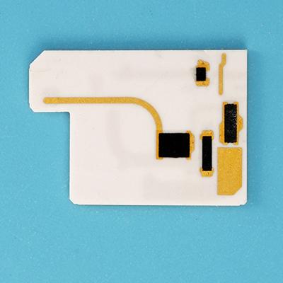
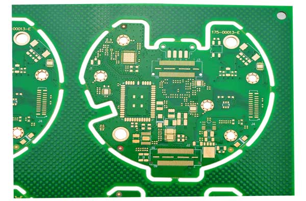
Board electronics with holes The types of vias in PCB include through holes, blind holes and buried holes, which have different characteristics and requirements in design and manufacturing. The selection of the appropriate via type should consider the number of PCB layers, wiring density, signal frequency, cost budget and production process. The via design should pay attention to avoid affecting the welding quality, preventing electrical short circuits, and saving costs in high-density packaging.
What are the holes in a PCB called?
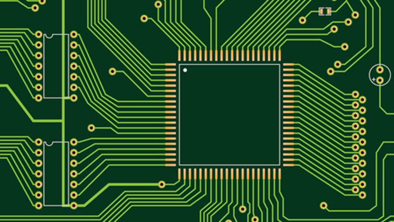
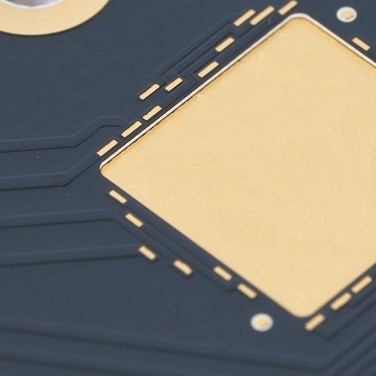
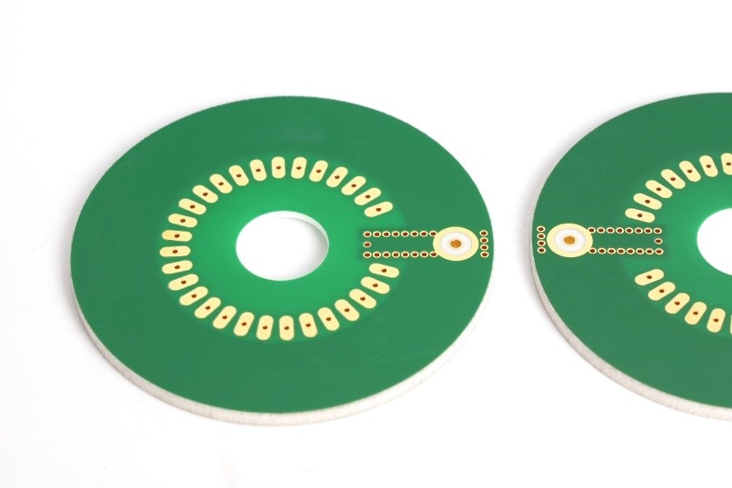
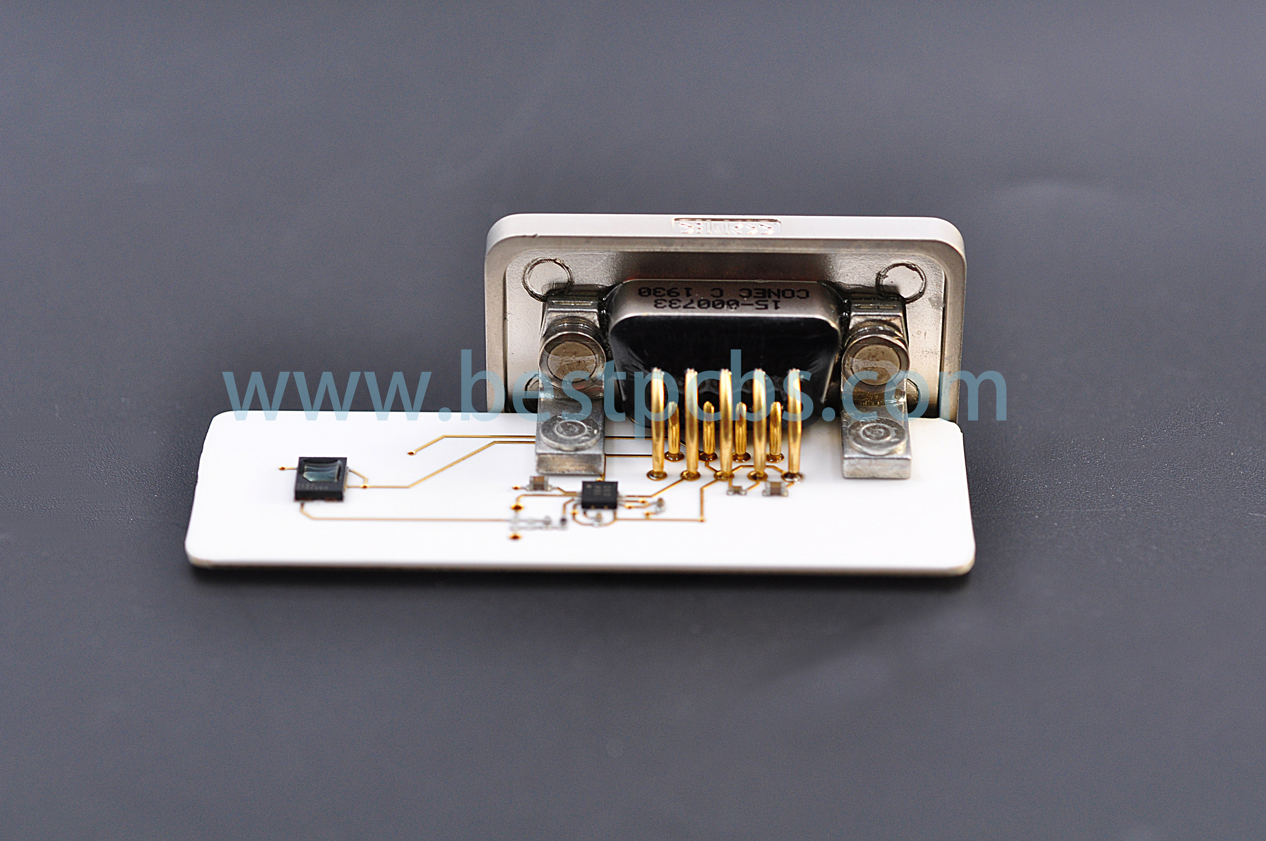
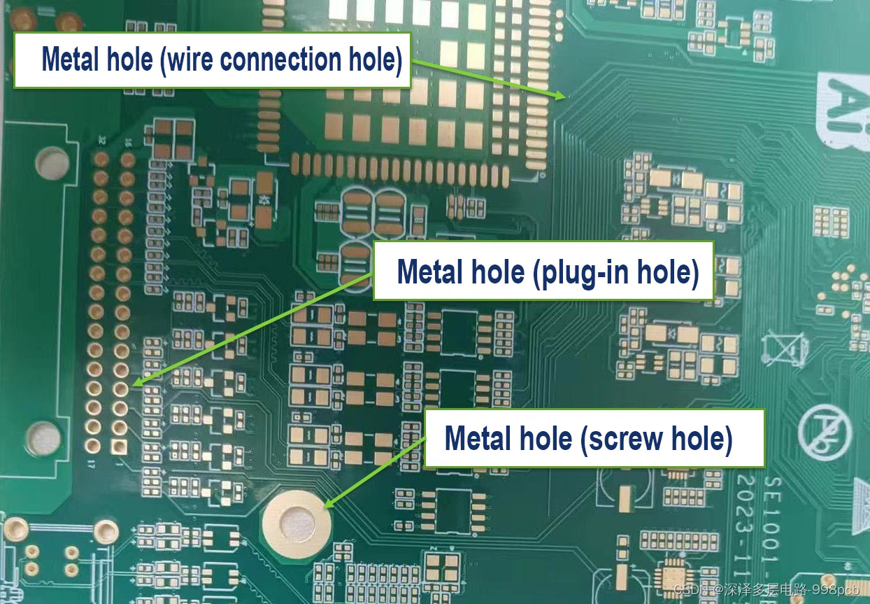
What are the holes on PCB called? What are the holes in the circuit? The holes on PCB can be roughly divided into 3 types, screw holes (mounting holes), conductive holes (vias), and plug-in holes.
Screw holes: Screw holes are used for fixing.
Conductive holes: Conductive holes (also called vias) are used for conducting electricity just like circuits.
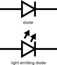
Plug-in holes: Plug-in holes are of course used to plug in various parts, such as diodes, transistors, capacitors, inductors, etc.
What is a through hole
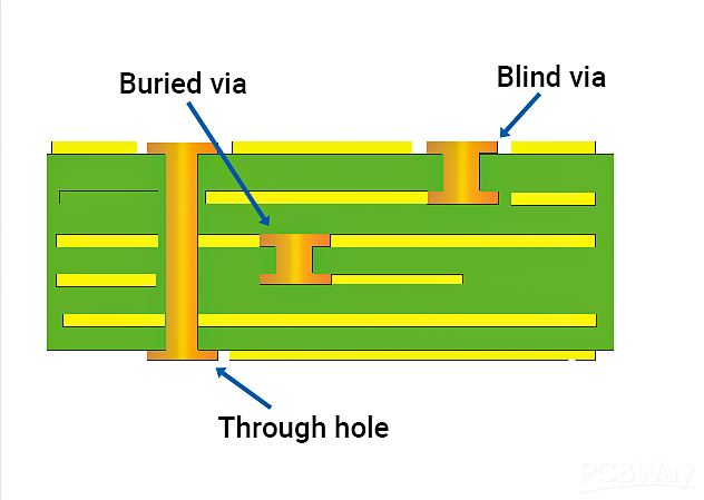
What is a through hole? Through holes, also known as perforations, are holes in a PCB that go all the way through the board. Their main purpose is to provide electrical connections for component pins while allowing soldering on both sides of the board.
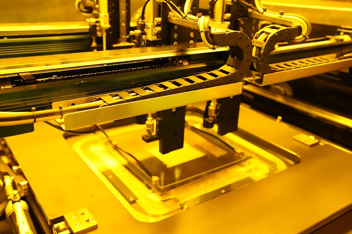
1.A via is a special through hole whose wall is metallized to achieve electrical connection between different layers on a circuit board. This type of hole is usually used to connect component pins to internal circuits, or to achieve electrical connection between different layers in a multi-layer PCB. Vias need to be metallized during the PCB manufacturing process, which usually includes drilling, desmearing, chemical copper plating, and electroplating.
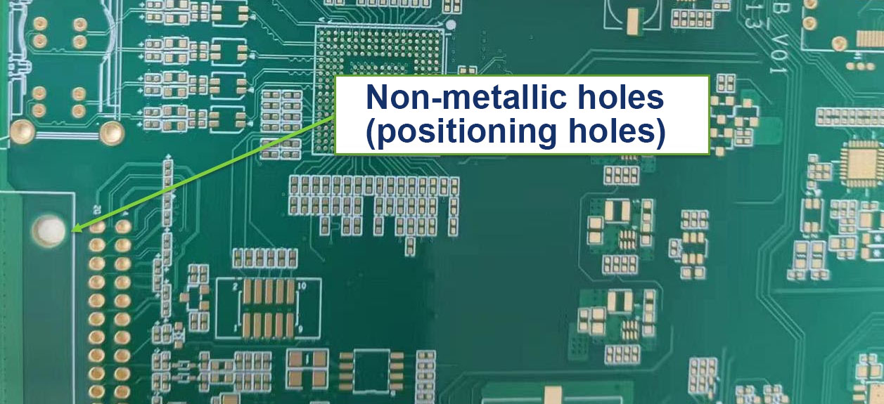
2.Non-conducting holes are the opposite of through holes. Their hole walls are not metallized, so they do not have electrical connection functions. These holes are mainly used for mechanical fixation, heat dissipation or identification purposes. Non-conducting holes are relatively simple in the PCB manufacturing process, and only drilling operations are required.
What is a blind via?
A blind via is a hole that extends from one side of a PCB to a certain internal layer without penetrating the entire board. The emergence of blind vias is mainly due to the development of HDI technology, which provides circuit designers with greater flexibility and more compact layout. Blind vias are usually used to connect surface mount components (SMD) to internal circuit layers, or to connect circuits between different internal layers.
What are buried vias?
Buried vias are holes located inside the PCB that do not penetrate any side of the board. They are completely hidden inside the board and are used to connect circuits between different internal layers. Buried vias are especially useful in HDI boards because they can reduce the overall thickness of the board while maintaining electrical connections between internal circuits.
What is a microvia?
Microvia refers to a hole with a smaller diameter, usually at the micron level. The emergence of microvia technology enables PCB designers to achieve more complex circuit layouts in a smaller space. Microvias are often used in high-density, high-reliability electronic devices such as mobile phones and tablets. The manufacture of microvias requires high-precision drilling equipment and technology to ensure the accuracy and reliability of the holes.
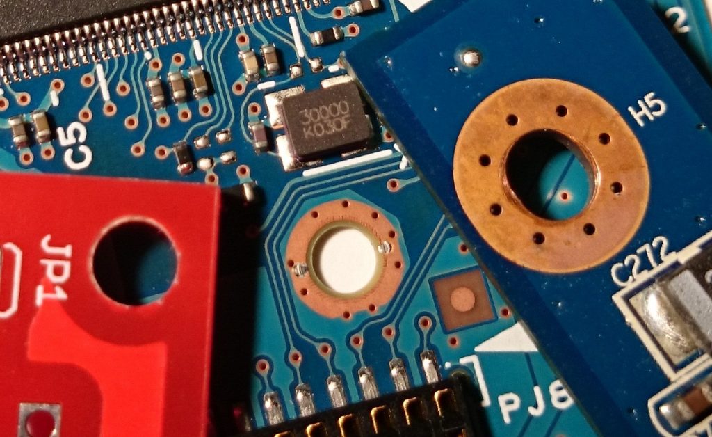
What are Mounting holes?
What are Mounting holes?Locking holes are auxiliary holes used in the PCB manufacturing and assembly process to accurately locate and fix the circuit board. They are usually located at the edge or specific position of the PCB to ensure that the circuit board can be accurately aligned and fixed during manufacturing, testing and assembly. The locating holes do not participate in the connection of the circuit, but are essential to ensure the quality and performance of the circuit board.
What are Mounting holes?
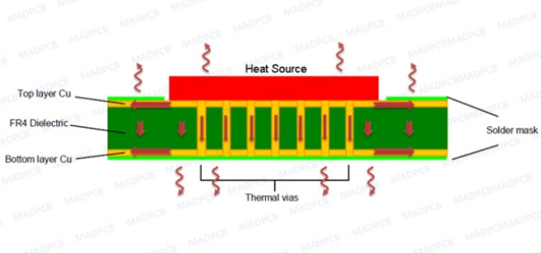
What are thermal vias?
Thermal vias are holes designed specifically for heat dissipation, usually large and can run through the entire PCB or multiple layers. Their role is to reduce heat buildup on the circuit board by increasing surface area and air flow, thereby improving the stability and reliability of the device. Thermal vias are particularly important in high-performance, high-power electronic devices.
FAQ About board electronics with holes
How to solve the contradiction between manual routing and automatic routing of high-speed signals?
Most of the current powerful routing software’s automatic routing tools have set constraints to control the routing method and the number of vias. The routing engine capabilities and constraint setting items of various EDA companies are sometimes very different. For example, whether there are enough constraints to control the winding method of the serpentine, whether the routing spacing of the differential pair can be controlled, etc. This will affect whether the routing method generated by automatic routing can meet the designer’s ideas. In addition, the difficulty of manually adjusting the routing is also related to the capabilities of the routing engine. For example, the pushing ability of the routing, the pushing ability of the via, and even the pushing ability of the routing pair copper. Therefore, choosing a routing tool with strong routing engine capabilities is the solution.
Will adding test points affect the quality of high-speed signals?
As for whether it will affect the signal quality, it depends on the method of adding test points and how fast the signal is. Basically, the additional test points (not using the existing vias (via or DIP pins) as test points) may be added to the line or a small section of wire may be pulled out from the line. The former is equivalent to adding a very small capacitor to the line, while the latter is an additional branch. Both of these situations will have some impact on high-speed signals, and the extent of the impact is related to the frequency speed of the signal and the edge rate of the signal. The magnitude of the impact can be learned through simulation. In principle, the smaller the test point, the better (of course, it must meet the requirements of the test equipment) and the shorter the branch, the better.
Can you introduce some foreign technical books and data on high-speed PCB design?
Now the application of high-speed digital circuits includes communication networks and calculators and other related fields. In the communication network, the operating frequency of PCB boards has reached around GHz, and the number of layers is as many as 40 layers as far as I know. Due to the advancement of chips, the operating frequency of calculator-related applications, whether it is a general PC or server, has reached 400MHz (such as Rambus) or above. In response to the demand for high-speed and high-density routing, the demand for blind/buried vias, mircrovias and build-up process technology is gradually increasing. These design requirements can be mass-produced by manufacturers.
Does the design of rigid-flexible boards require special design software and specifications? Where can I undertake the processing of such circuit boards in China?
Can I use general PCB design software to design flexible printed circuits (Flexible Printed Circuit). The Gerber format is also used for FPC manufacturers to produce. Since the manufacturing process is different from that of general PCBs, each manufacturer will have its own restrictions on line width, line spacing, and aperture (via) based on their manufacturing capabilities. In addition, some copper foil can be laid at the turning point of the flexible circuit board for reinforcement. As for the manufacturer, you can search for “FPC” as a keyword on the Internet and you should be able to find it.
If the size of the circuit board is fixed, if the design needs to accommodate more functions, it is often necessary to increase the routing density of the PCB, but this may lead to increased mutual interference between the routings, and at the same time, the impedance cannot be reduced if the routing is too thin. Please introduce the techniques in the design of high-speed (>100MHz) high-density PCBs?
When designing high-speed and high-density PCBs, crosstalk interference does need to be paid special attention to because it has a great impact on timing and signal integrity. Here are a few things to note:
Control the continuity and matching of the characteristic impedance of the trace.
The size of the trace spacing. The spacing commonly seen is twice the line width. Through simulation, you can know the impact of trace spacing on timing and signal integrity and find the tolerable spacing. The results of different chip signals may be different.
Choose an appropriate termination method.
Avoid the same routing direction of the upper and lower adjacent layers, or even have traces overlapped up and down, because this kind of crosstalk is greater than the case of adjacent traces on the same layer.
Use blind/buried vias to increase the trace area. However, the production cost of the PCB board will increase. It is indeed difficult to achieve complete parallelism and equal length in actual implementation, but it should be done as much as possible.
In addition, differential termination and common mode termination can be reserved to mitigate the impact on timing and signal integrity.
The RF part, IF part, and even the low-frequency circuit part of the outdoor unit are often deployed on the same PCB. What are the material requirements for such PCB? How to prevent interference between RF, IF, and even low-frequency circuits?
Hybrid circuit design is a big problem. It is difficult to have a perfect solution.
Generally, RF circuits are laid out and wired as an independent single board in the system, and there will even be a special shielding cavity. Moreover, RF circuits are generally single-sided or double-sided boards, and the circuits are relatively simple. All of these are to reduce the impact on the distributed parameters of RF circuits and improve the consistency of RF systems. Compared with general FR4 materials, RF circuit boards tend to use high-Q substrates. The dielectric constant of this material is relatively small, the distributed capacitance of the transmission line is small, the impedance is high, and the signal transmission delay is small. In hybrid circuit design, although RF and digital circuits are made on the same PCB, they are generally divided into RF circuit area and digital circuit area, and laid out and wired separately. Shielding is used between ground vias and shielding boxes.