Archive for May, 2023

5 Tips Tell You How to Solder BGA Better in PCBA

Monday, May 29th, 2023

BGA (Ball Grid Array) soldering is a widely used method in the electronics manufacturing industry for mounting integrated circuits onto printed circuit boards (PCBs). This method provides a more compact and reliable connection compared to traditional through-hole or surface mount technology (SMT). However, the complexity of BGA soldering poses various obstacles during the manufacturing process. Herein, we will explore the challenges faced in BGA soldering and discuss effective strategies to address them.

What is BGA Soldering?

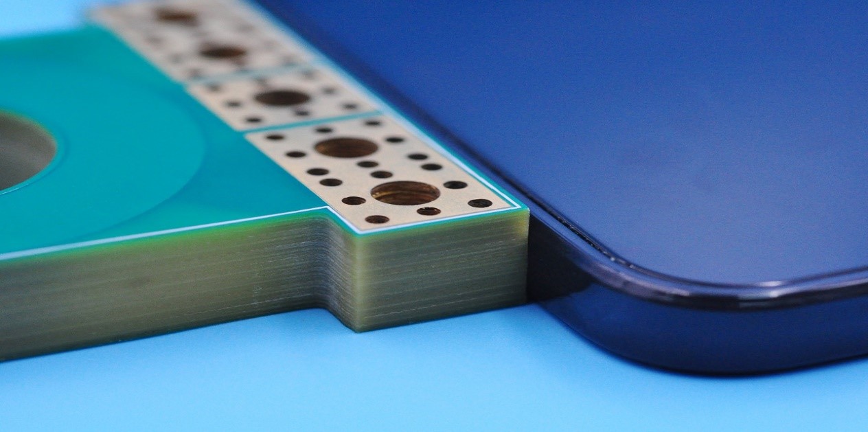
BGA soldering is a technique that involves the attachment of integrated circuit packages to a PCB using an array of solder balls. These solder balls are typically made of lead-based or lead-free alloys, depending on environmental regulations and specific requirements. The BGA package consists of a substrate, which acts as a carrier for the integrated circuit, and the solder balls that form the electrical and mechanical connections between the package and the PCB.

(BGA_balls)

The Importance of BGA Soldering in Electronics Manufacturing

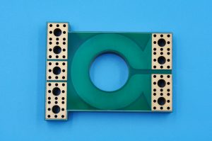
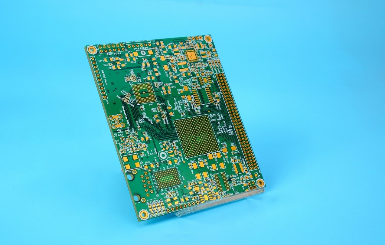
BGA soldering plays a critical role in the manufacturing of various electronic devices such as computers, smartphones, and gaming consoles. The increased demand for smaller and more powerful electronics has driven the adoption of BGA packages. Their compact size and high pin density make them suitable for advanced applications where space is limited.

Challenges Faced in BGA Soldering

  • Component Alignment and Placement

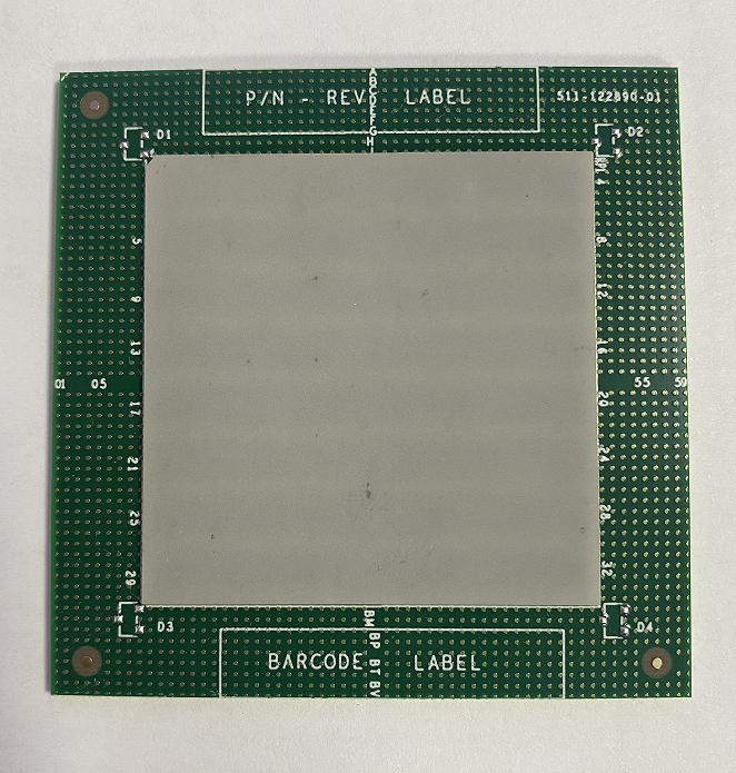
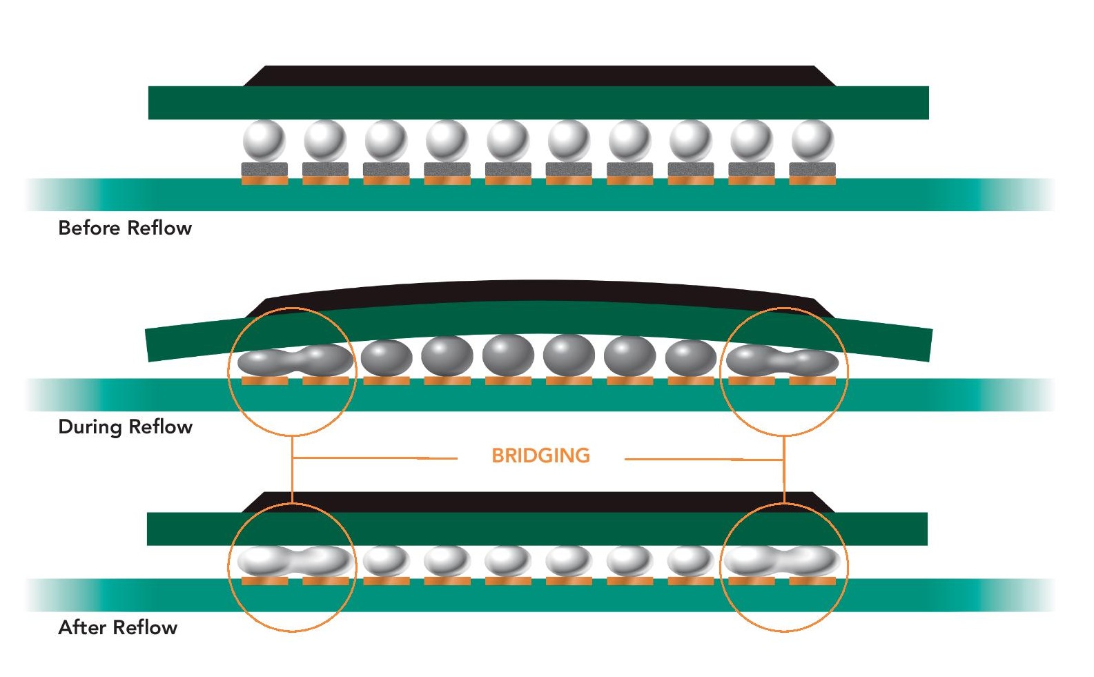
One of the primary challenges in BGA soldering is ensuring accurate component alignment and placement on the PCB. The small size of the solder balls and the dense layout of the BGA package make it difficult to achieve precise positioning. Misalignment during the assembly process can result in solder bridges, open connections, or mechanical stress on the package.

To address this challenge, manufacturers employ advanced technologies such as Automated Optical Inspection (AOI) and X-ray Inspection. AOI systems use cameras and image processing algorithms to verify the correct alignment and placement of BGA components. X-ray inspection, on the other hand, allows manufacturers to see beneath the surface of the PCB and detect any misalignment or defects that may not be visible to the naked eye.

(Alignment)
  • Solder Paste Application

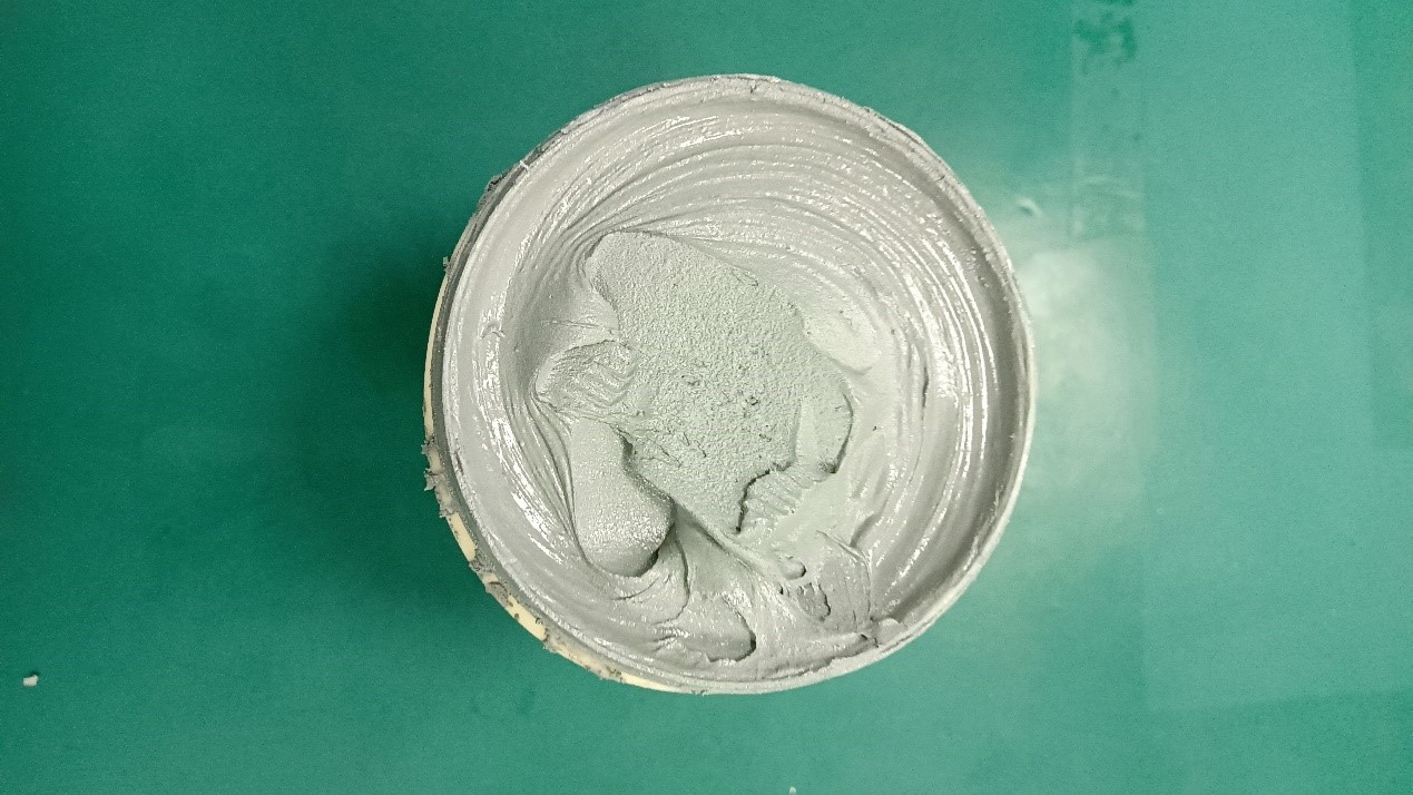
Another significant challenge in BGA soldering is achieving precise and consistent solder paste application. Solder paste, a mixture of solder alloy and flux, is applied to the PCB pads before placing the BGA package. Inadequate or excessive solder paste can lead to solder defects such as insufficient solder joints, solder voids, or solder bridging.

To overcome this challenge, careful attention must be given to stencil design and aperture selection. Stencils with appropriate thickness and properly sized apertures ensure accurate solder paste deposition. Additionally, manufacturers can employ Solder Paste Inspection (SPI) systems to verify the quality and consistency of the solder paste applied. The solder paste that Best Technology uses is SAC305 solder paste, which has good printability and excellent stability.

(SAC305_Solder_paste)
  • Temperature Profiling

Temperature profiling, or we can say the thermal management, it is crucial in BGA soldering to ensure proper reflow of the solder paste. The reflow process involves subjecting the PCB to a carefully controlled temperature profile, allowing the solder paste to melt, form a reliable joint, and solidify. Inadequate temperature profiling can lead to insufficient solder wetting, incomplete reflow, or thermal damage to components.

Manufacturers must optimize the reflow oven setup and calibration to achieve the correct temperature profile. Thermal profiling techniques, such as the use of thermocouples and data loggers, help monitor and control the temperature during the reflow process.

  • Reflow Process

The reflow process itself presents challenges in BGA soldering. The soak zone, ramp rates, and peak temperature must be carefully controlled to prevent thermal stress on the components and ensure proper solder reflow. Inadequate temperature control or improper ramp rates can result in solder defects such as tombstoning, component warpage, or voids in the solder joints.

Manufacturers need to consider the specific requirements of the BGA package and follow recommended reflow profiles provided by component suppliers. Proper cooling after reflow is also essential to prevent thermal shock and ensure the stability of the solder joints.

(BGA_reflow)
  • Inspection and Quality Control

Inspection and quality control are critical aspects of BGA soldering to ensure the reliability and performance of the solder joints. Automated Optical Inspection (AOI) systems and X-ray inspection are commonly used to detect defects such as misalignment, insufficient solder wetting, solder bridging, or voids in the solder joints.

(AOI)

In addition to visual inspection techniques, some manufacturers may perform cross-section analysis, where a sample solder joint is cut and examined under a microscope. This analysis provides valuable information about the quality of the solder joint, such as solder wetting, void formation, or the presence of intermetallic compounds.

In a word, BGA soldering presents unique challenges in electronics manufacturing, primarily related to various factors. By addressing these challenges effectively, manufacturers can ensure the reliability and performance of BGA solder joints, contributing to the production of high-quality electronic devices. Best Technology has rich experience in PCBA assembly and we mounted thousands PCBs for our customers, whatever it is simple design or complex design, all the products are assemble perfect and work well in customer side. Please feel free to contact us for any questions about PCBA.

You may also like

Key Challenges in Solder Mask Printing for Heavy Copper PCBs

Tuesday, May 23rd, 2023

As the demand for higher power and miniaturization of electronics increases, so does the need for Heavy Copper Printed Circuit Boards (PCBs). From our last blog – Why choose Heavy Copper PCB for your High Current Project, we know the heavy copper PCBs are defined as those with copper thicknesses greater than 3 oz. These PCBs are designed to withstand high current and thermal loads, making them suitable for power electronics applications. However, the increased copper thickness also poses challenges during the solder mask printing process.

(16_layers_heavy_copper_PCB_with_10oz_each_layer)

Understanding solder mask

Solder mask (short for S/M in the industry) is a protective coating applied to PCBs to prevent solder bridges and improve solder joint quality. The solder mask is coated to the PCB surface using a screen-printing process, where the desired pattern is created using a stencil and the solder mask ink is then deposited onto the PCB. The ink is then cured, either through heat baking or UV light, to form a solid coating.

There are several types of solder mask materials available, including epoxy, acrylic, and liquid photo imageable (LPI) solder mask. Each type has its advantages and disadvantages, depending on the application requirements.

The benefits of using solder mask in PCB manufacturing include increased reliability, improved solderability, and reduced risk of short circuits and corrosion. The solder mask we usually use is Taiyo, which has high reliability and excellent heat resistance.

(Solder_mask_manually_printing)

Challenges in solder mask printing of heavy copper PCBs

While solder mask printing is a critical step in PCB manufacturing, the increased copper thickness in heavy copper PCBs presents several challenges for printing process as I mentioned before. It’s difficult to apply enough solder mask to cover thick copper pattern and base material with severe height difference.

1. The high copper thickness and thermal conductivity of heavy copper PCBs make it difficult for the solder mask ink to adhere properly to the surface. This can result in insufficient coverage and registration accuracy, which can affect the overall quality and reliability of the PCB.

2. The high copper thickness can cause stress on the solder mask, leading to mask cracking and peeling. The navigation mark on the substrate has specific ink thickness requirements due to limitations in the ink thickness that can be applied to the substrate. If the ink thickness on the substrate is too thick, it may result in solder resist cracks in the substrate position after the printed circuit board is soldered. This can occur during reflow soldering or thermal cycling, resulting in poor solder joint quality and reduced reliability.

3. The thick solder mask is also more difficult to exposure and develop. If the exposure energy is too weak or not enough, then some undercut problem may happen.

How to overcome this challenge?

To address these challenges, it is essential to choose the right solder mask materials and optimize the application process.

  • Choosing the right solder mask materials is crucial for ensuring proper adhesion and coverage on heavy copper PCBs. LPI solder mask is often preferred for heavy copper PCBs due to its excellent adhesion and thermal stability. However, epoxy and acrylic solder mask materials can also be used with proper surface preparation.
  • Optimizing the solder mask application process can also help address the challenges of heavy copper PCBs. This can include using a thinner stencil for improved registration accuracy and applying multiple coats of solder mask for better coverage. Advanced solder mask technology, such as laser direct imaging (LDI), can also help improve registration accuracy and reduce the risk of mask cracking and peeling.
  • Optimizing the printing process, now in Best Technology, we always make the substrate first, fill the substrate with the solder mask and then treat it as a normal PCB for normal printing solder mask.
(Solder_mask_printing)

If you are in the process of designing a complex multi-layer heavy copper PCB and are looking for a high-quality and experienced manufacturer, feel free to reach out to us at sales@bestpcbs.com, Best Technology can support you by OEM and ODM service to ensure your design is cost-effective and can be easily manufactured.

You may also like

Why choose Heavy Copper PCB for your High Current Project?

Tuesday, May 16th, 2023

In the world of electronics, printed circuit boards (PCBs) play a vital role in connecting and powering various components. They are the backbone of every electronic device, from smartphones to industrial machinery. When it comes to designing a PCB for a project, the thickness of the copper layer is an important consideration. Heavy Copper PCB, also known as Thick Copper PCB, has become increasingly popular in charging automotives due to their unique features and benefits. In this article, we will discuss why consider heavy copper PCBs for your high current project.

What a Heavy Copper PCB is?

A heavy copper PCB is a circuit board with an unusually thick copper layer, usually exceeding 3 ounces per square foot (oz/ft²). By comparison, standard PCBs typically have a copper layer thickness of 1 oz/ft². Heavy copper PCBs are used in applications where high current is needed, or the board needs to withstand mechanical and thermal stress.

(Heavy_copper_PCB)

Benefits of Heavy Copper PCBs

  • High Current Capacity

The thicker copper layer in a heavy copper PCB allows for a higher current capacity. This makes it ideal for high-power applications such as power supplies, motor controllers, and industrial equipment. Heavy copper PCBs can carry up to 20 amps or more, compared to the standard 5-10 amps of a regular PCB.

  • Thermal Management

Heavy copper PCBs are known for their excellent thermal management capabilities. The thicker copper layer allows for better heat dissipation, reducing the risk of overheating and component failure. So that they can generate a lot of heat for the end-application.

  • Durability

Heavy copper PCBs are more robust and durable than standard PCBs. The thicker copper layer provides better mechanical support, making them resistant to damage from vibration, shock, and bending. This makes them suitable for harsh environments and industrial applications.

  • Increased Flexibility

Heavy copper PCBs offer increased design flexibility compared to standard PCBs. The thicker copper layer allows for more complex and compact designs, reducing the overall size of the board. This makes them ideal for applications where space is limited, that means you can make a very heavy copper while the size is very small.

  • Better Signal Integrity

The thicker copper layer in heavy copper PCBs provides better signal integrity. This reduces the risk of signal loss and interference, resulting in more reliable and efficient circuit performance.

Copper thickness design for a Heavy Copper PCB?

Due to the thickness of copper in heavy copper PCB is thick then normal FR4 PCB, then it is easily to be warped if the copper thickness is not match each other in symmetrical layers. For example, if you are designing an 8 layers heavy copper PCB, then the copper thickness in each layer should follow L8=L1, L7=L2, L6=L3, L5=L4 standard.

Additionally, the relationship between minimum line space and minimum line width also should be considered, follow the design rule will help to smooth production and shorten the lead time. Below are the design rules between them, LS refers to line space and LW refers to line width.

(Heavy_copper_design_rule)

Drill hole rules for heavy copper board

A plated through hole (PTH) in printed circuit board is to connect top and bottom side to make them electricity. And when the PCB design has multi copper layers, the parameters of holes must be considered carefully, especially hole diameters.

In Best Technology, the minimum PTH diameter should be >=0.3mm while the copper ring annular should be 0.15mm at least. For wall copper thickness of PTH, 20um-25um as default, and maximum 2-5OZ (50-100um).

(16L_heavy_copper_PCB_with_35um_copper_in_via_holes)

Basic parameters of Heavy Copper PCB

Here are some basic parameters of heavy copper PCB, hope this can help you to understand Best Technology’s capability better.

  • Base material: FR4
  • Copper thickness: 4 OZ~30 OZ
  • Extreme Heavy Copper: 20~200 OZ
  • Outline: Routing, punching, V-Cut
  • Solder mask: White/Black/Blue/Green/Red Oil (Solder mask printing is not easy in heavy copper PCB.)
  • Surface finishing: Immersion Gold, HASL, OSP
  • Max Panel size: 580*480mm (22.8″*18.9″)

Applications of Heavy Copper PCBs

Heavy copper PCBs are used in a variety of applications, including:

  • Power supplies
  • Motor controllers
  • Industrial machinery
  • Automotive electronics
  • Aerospace and defense systems
  • Solar inverters
  • LED lighting
(Heavy_copper_PCB_for_high_power_supply)

Choosing the right PCB thickness is crucial for the success of any project. Heavy copper PCBs offer unique features and benefits that make them ideal for high-power and high-temperature applications. If you want to ensure the reliability and performance of your project, consider using heavy copper PCBs. Best Technology has more than 16 years manufacturing experience in heavy copper PCBs, so we are so confident that we can be your most reliable supplier in China. Welcome to contact us at any time for any questions or any queries about PCBs.

You may also like