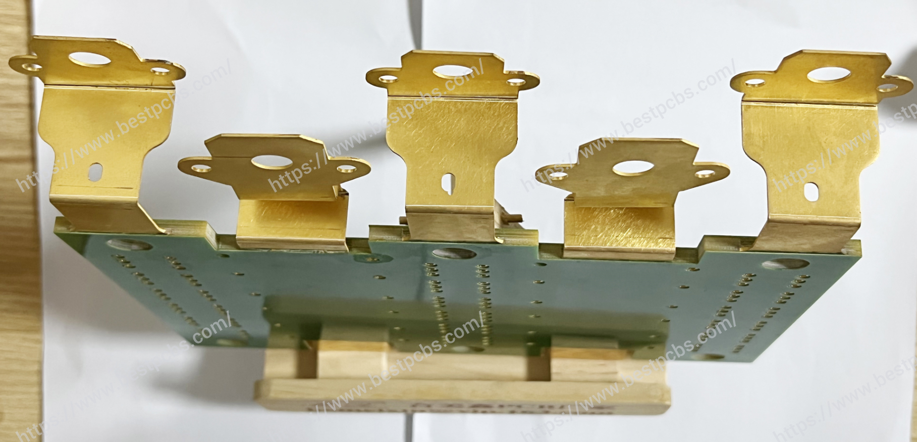
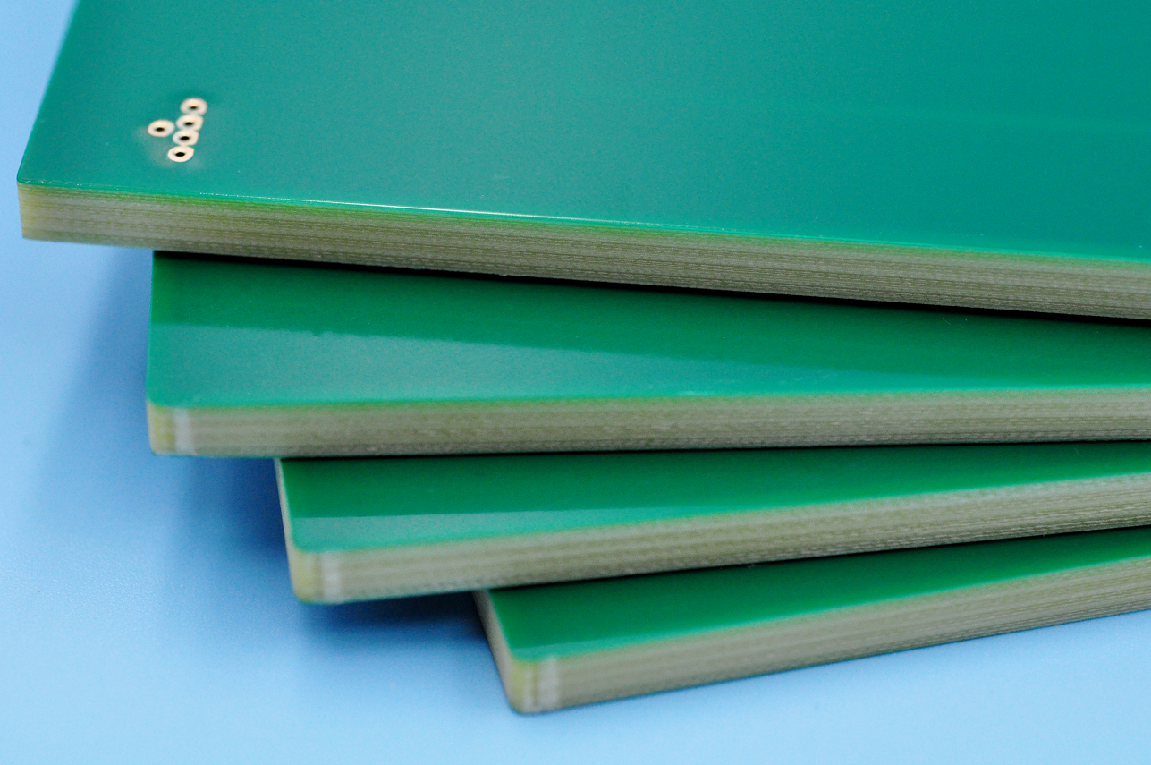
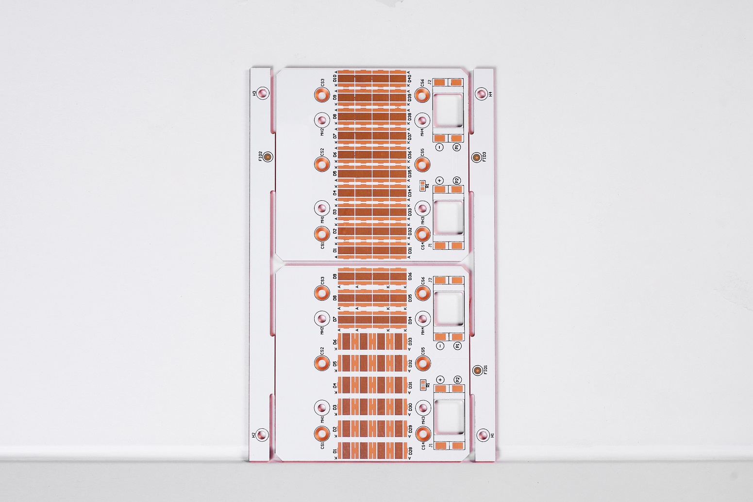
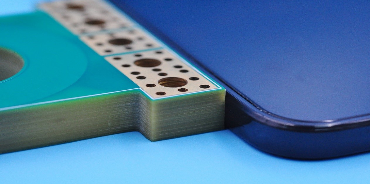
As the demand for higher power and miniaturization of electronics increases, so does the need for Heavy Copper Printed Circuit Boards (PCBs). From our last blog – Why choose Heavy Copper PCB for your High Current Project, we know the heavy copper PCBs are defined as those with copper thicknesses greater than 3 oz. These PCBs are designed to withstand high current and thermal loads, making them suitable for power electronics applications. However, the increased copper thickness also poses challenges during the solder mask printing process.
Understanding solder mask
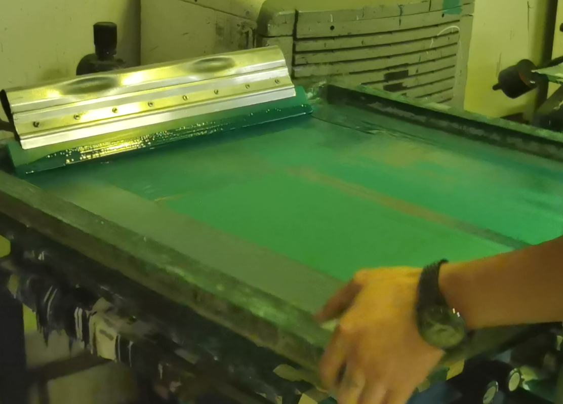
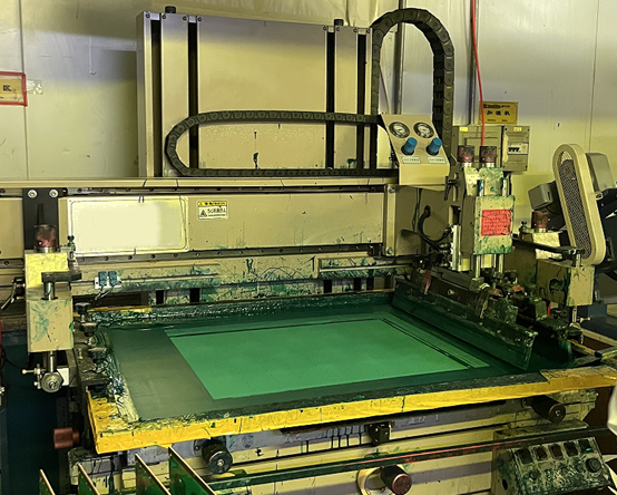
Solder mask (short for S/M in the industry) is a protective coating applied to PCBs to prevent solder bridges and improve solder joint quality. The solder mask is coated to the PCB surface using a screen-printing process, where the desired pattern is created using a stencil and the solder mask ink is then deposited onto the PCB. The ink is then cured, either through heat baking or UV light, to form a solid coating.
There are several types of solder mask materials available, including epoxy, acrylic, and liquid photo imageable (LPI) solder mask. Each type has its advantages and disadvantages, depending on the application requirements.
The benefits of using solder mask in PCB manufacturing include increased reliability, improved solderability, and reduced risk of short circuits and corrosion. The solder mask we usually use is Taiyo, which has high reliability and excellent heat resistance.
Challenges in solder mask printing of heavy copper PCBs
While solder mask printing is a critical step in PCB manufacturing, the increased copper thickness in heavy copper PCBs presents several challenges for printing process as I mentioned before. It’s difficult to apply enough solder mask to cover thick copper pattern and base material with severe height difference.
1. The high copper thickness and thermal conductivity of heavy copper PCBs make it difficult for the solder mask ink to adhere properly to the surface. This can result in insufficient coverage and registration accuracy, which can affect the overall quality and reliability of the PCB.
2. The high copper thickness can cause stress on the solder mask, leading to mask cracking and peeling. The navigation mark on the substrate has specific ink thickness requirements due to limitations in the ink thickness that can be applied to the substrate. If the ink thickness on the substrate is too thick, it may result in solder resist cracks in the substrate position after the printed circuit board is soldered. This can occur during reflow soldering or thermal cycling, resulting in poor solder joint quality and reduced reliability.
3. The thick solder mask is also more difficult to exposure and develop. If the exposure energy is too weak or not enough, then some undercut problem may happen.
How to overcome this challenge?
To address these challenges, it is essential to choose the right solder mask materials and optimize the application process.
- Choosing the right solder mask materials is crucial for ensuring proper adhesion and coverage on heavy copper PCBs. LPI solder mask is often preferred for heavy copper PCBs due to its excellent adhesion and thermal stability. However, epoxy and acrylic solder mask materials can also be used with proper surface preparation.
- Optimizing the solder mask application process can also help address the challenges of heavy copper PCBs. This can include using a thinner stencil for improved registration accuracy and applying multiple coats of solder mask for better coverage. Advanced solder mask technology, such as laser direct imaging (LDI), can also help improve registration accuracy and reduce the risk of mask cracking and peeling.
- Optimizing the printing process, now in Best Technology, we always make the substrate first, fill the substrate with the solder mask and then treat it as a normal PCB for normal printing solder mask.
If you are in the process of designing a complex multi-layer heavy copper PCB and are looking for a high-quality and experienced manufacturer, feel free to reach out to us at sales@bestpcbs.com, Best Technology can support you by OEM and ODM service to ensure your design is cost-effective and can be easily manufactured.
Tags: heavy copper pcb, solder mask
