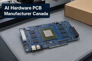
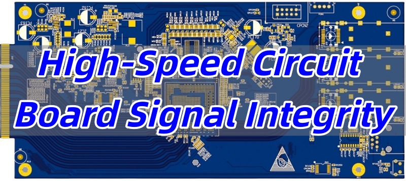
AI accelerator PCB combines fast data channels, high current, dense packages, and demanding thermal interfaces on one board. A weakness in the stackup, via structure, material choice, assembly process, or inspection plan can cause signal loss, unstable power, solder defects, overheating, or an expensive redesign.
EBest Circuit (Best Technology) supports these projects from manufacturability review and material coordination through PCB fabrication, component sourcing, BGA assembly, X-ray inspection, and customer-defined testing. Keeping these stages with one manufacturing partner helps maintain the same revision, stackup, component, and quality requirements from prototype to repeat production.
If you are preparing an AI accelerator PCB for quotation or production, send your Gerber data, stackup, BOM, assembly files, and test requirements to sales@bestpcbs.com for a project-specific review.
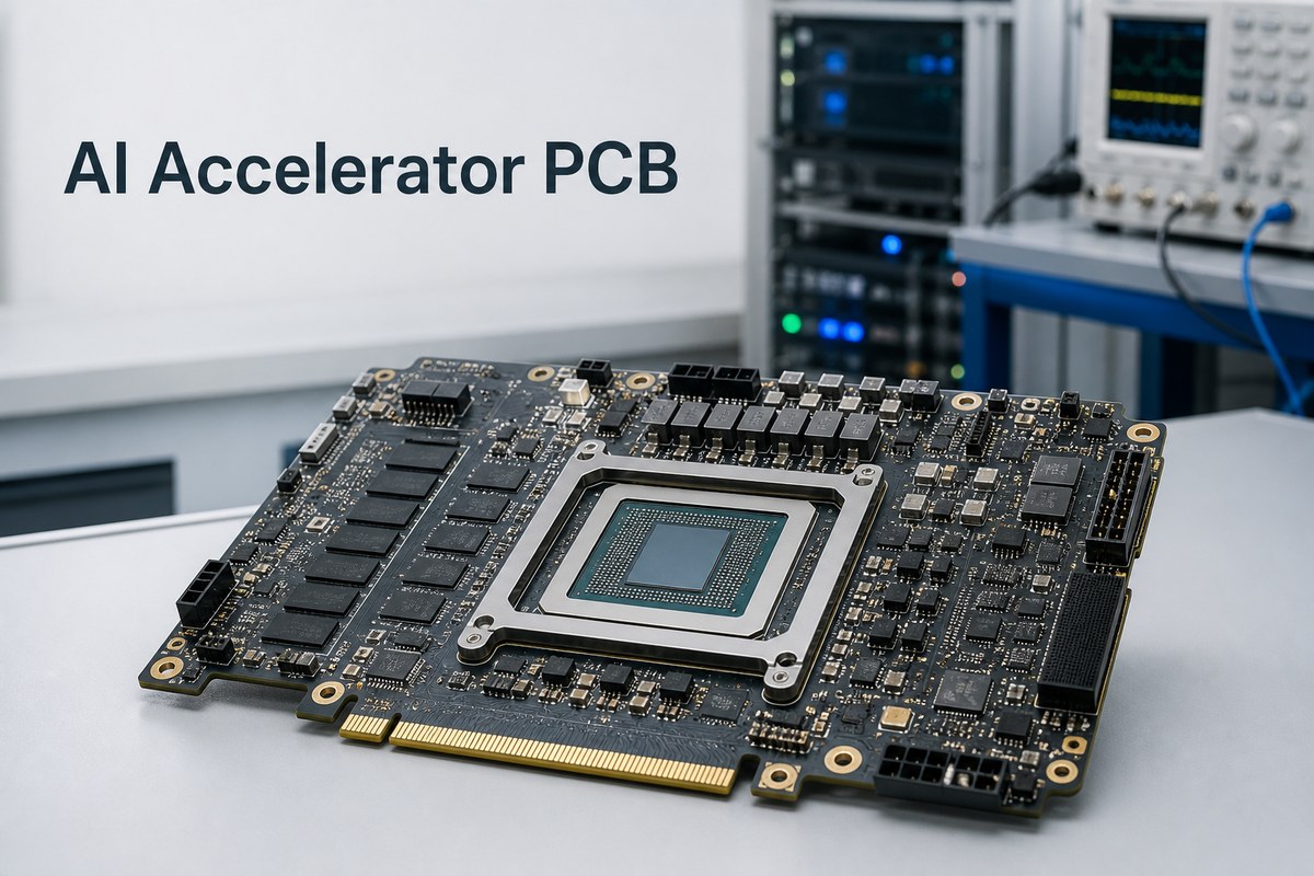
What Is an AI Accelerator PCB?
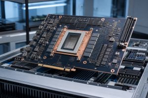
An AI accelerator PCB is the circuit board that carries or connects specialized processors used to accelerate artificial-intelligence workloads. The processor may be a GPU, NPU, ASIC, FPGA, or another dedicated computing device.
The PCB provides the physical platform for:
- High-speed connections to the host, memory, and other accelerators.
- Stable power for the processor, memory, and supporting circuits.
- Management, clock, control, and communication devices.
- Mechanical attachment to connectors, stiffeners, heatsinks, and the enclosure.
- Component assembly, inspection, programming, and testing.
Depending on the system, the product may be a PCIe accelerator card, an embedded AI module, an OAM-style module, a carrier or baseboard, or a custom computing assembly. The PCB is not the accelerator chip itself; it is the high-density electrical and mechanical foundation that allows the accelerator to operate inside the finished product.
What Are the Key Requirements for AI Accelerator PCBs?
An effective AI accelerator PCB must handle high-speed data, high current, dense interconnection, thermal stress, and reliable assembly at the same time.
The main requirements are:
- Controlled high-speed channels: The stackup, impedance, routing layers, vias, and connectors must support the customer’s channel targets.
- Stable power delivery: Power and ground structures must carry the required current without excessive voltage drop or localized heating.
- Suitable PCB materials: Laminates, copper profiles, and dielectric thicknesses must match signal-loss, thermal, mechanical, availability, and cost needs.
- High-density routing: Fine-pitch devices and connectors may require HDI, blind or buried vias, via-in-pad, or back drilling.
- Thermal and mechanical compatibility: Board thickness, copper distribution, mounting holes, stiffeners, and heatsink interfaces must work together.
- Repeatable PCBA: Stencil design, component handling, placement, reflow, warpage control, and inspection must suit large or fine-pitch packages.
- Defined quality evidence: Bare-board tests, AOI, X-ray, electrical tests, and functional tests should match the risks of the product.
These requirements are interdependent. Increasing copper for power, for example, can change etching, lamination, impedance geometry, reflow behavior, and board flatness. The best result comes from reviewing the complete board rather than treating each specification separately.
Why Are AI Accelerator PCBs Difficult to Manufacture?
AI accelerator PCBs are difficult to manufacture because several advanced features often appear on the same board, leaving less room for process variation.
Common combinations that increase difficulty include:
- Many signal, power, and ground layers in a controlled finished thickness.
- Low-loss materials combined with fine traces and tight impedance control.
- Blind, buried, stacked, filled, or back-drilled vias.
- Dense accelerator, memory, and connector breakout areas.
- Large copper areas next to fine-pitch circuitry.
- Large BGAs or modules with high thermal mass and warpage sensitivity.
A thicker multilayer board may improve routing and power distribution but make small-hole plating more difficult. Thin HDI dielectrics may improve package escape but require additional lamination cycles. Heavy copper can carry more current but may affect copper balance, etching, and assembly heat.
The challenge is therefore not simply producing one advanced feature. It is controlling registration, plating, lamination, impedance, flatness, and assembly when all those features interact. Early engineering review helps identify which combination is likely to control yield, cost, and lead time before material is committed.
What Stackup and Materials Are Used for AI Accelerator PCBs?
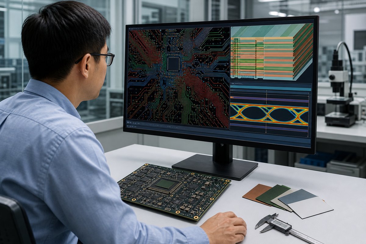
AI accelerator PCBs typically use multilayer or HDI stackups with dedicated signal, reference, power, and ground layers. The exact construction depends on channel length, interface speed, routing density, power demand, via architecture, board thickness, and mechanical form factor.
A practical stackup may include:
- Signal layers placed next to continuous reference planes.
- Closely coupled power and ground layers where required by the power-integrity design.
- HDI build-up layers for dense package or connector escape.
- Mechanically drilled through-holes for lower-density connections and structural strength.
- Back drilling where unused plated-through-hole stubs would create excessive signal discontinuity.
Low-loss materials are often used for long or fast channels, while hybrid stackups may place higher-performance material only where it provides a clear electrical benefit. Material selection should consider more than a published Dk or Df value.
| Decision | Customer priority | Manufacturing effect |
|---|---|---|
| Signal layers | Loss and impedance | Layer count and dielectric geometry |
| Power layers | Current and voltage drop | Copper weight and balance |
| Via structure | Package escape and stub limits | Drill and lamination sequence |
| Laminate | Electrical and thermal needs | Availability, processing, and cost |
| Thickness | Connector and mechanical fit | Stackup tolerance and flatness |
The production stackup should identify actual materials, dielectric thicknesses, finished copper, via structures, controlled impedances, and tolerances. If the fabricator proposes a material or geometry change, the customer’s electrical owner should evaluate its effect before the design is built.
What High-Speed Requirements Affect AI Accelerator PCB Manufacturing?
High-speed requirements affect material selection, stackup geometry, copper profile, impedance control, via design, back drilling, and fabrication tolerances.
Three areas deserve particular attention:
- Channel loss: Laminate loss, copper roughness, trace length, and via transitions determine how much of the signal reaches the receiver.
- Impedance discontinuity: Neck-downs, antipads, connectors, layer changes, and unused via stubs can create reflections.
- Skew and crosstalk: Pair geometry, reference planes, glass weave, spacing, and routing consistency affect timing and noise.
The fabrication drawing should clearly identify controlled-impedance structures, target values and tolerances, coupon requirements, and any back-drill or residual-stub limits. The fabricator should calculate impedance using the proposed production materials and finished copper rather than generic design values.
TDR coupon results can show whether selected structures meet the agreed impedance requirement. They do not replace the customer’s full-channel simulation, eye-diagram analysis, or protocol validation. The manufacturing value is consistency: the built geometry and test evidence should match the approved stackup.
What Power Requirements Affect AI Accelerator PCB Manufacturing?
AI accelerator PCB manufacturing must support high current, rapid load changes, low-voltage rails, and concentrated heat without creating excessive voltage drop or unreliable copper structures.
Board-level power affects:
- The number and location of power and ground layers.
- Copper weight, plane shape, neck-down areas, and connector transitions.
- The quantity and arrangement of power and thermal vias.
- Decoupling-component placement and available routing space.
- PCB thickness, copper balance, flatness, and assembly heat.
- Heatsink, stiffener, mounting, and airflow interfaces.
Even a short narrow section in a high-current path can create voltage drop and local heating. Likewise, adding heavy copper without considering balance can make fabrication and reflow less uniform. Power integrity therefore needs to be translated into practical plane geometry, copper construction, and via structures before the stackup is finalized.
EBest Circuit can review whether the released copper, via, material, and mechanical features are manufacturable. The customer or its design partner remains responsible for load assumptions, voltage-drop limits, simulation targets, and final cooling-system performance.
Why Is HDI Important for AI Accelerator PCBs?
HDI is important because dense accelerator packages and high-pin-count connectors can require smaller vias and more routing space than conventional through-hole structures provide.
HDI can help by:
- Escaping fine-pitch packages with shorter, smaller interconnects.
- Keeping through-holes from blocking multiple inner routing layers.
- Providing more direct access to power and ground structures.
- Reducing the electrical length of selected layer transitions.
- Supporting compact modules and dense connector areas.
However, HDI should not be added simply because the product is an AI board. Blind microvias, stacked structures, via-in-pad, copper filling, and repeated sequential lamination increase cost and process sensitivity. A staggered structure or a combination of microvias and mechanically drilled vias may be more practical when routing allows it.
The objective is the least complex via architecture that still meets package escape, signal, power, reliability, thickness, and cost requirements. Microvia depth, diameter, land size, stacking, filling, registration, and reliability expectations should be reviewed as one structure.
What Makes AI Accelerator PCB Assembly Difficult?
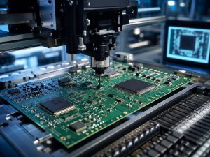
AI accelerator PCB assembly is difficult because large devices, fine-pitch joints, high component density, heavy copper, and uneven thermal mass must pass through one stable assembly process.
Major assembly risks include:
- BGA warpage: A large package and the PCB may bend differently during reflow, increasing open-joint or head-in-pillow risk.
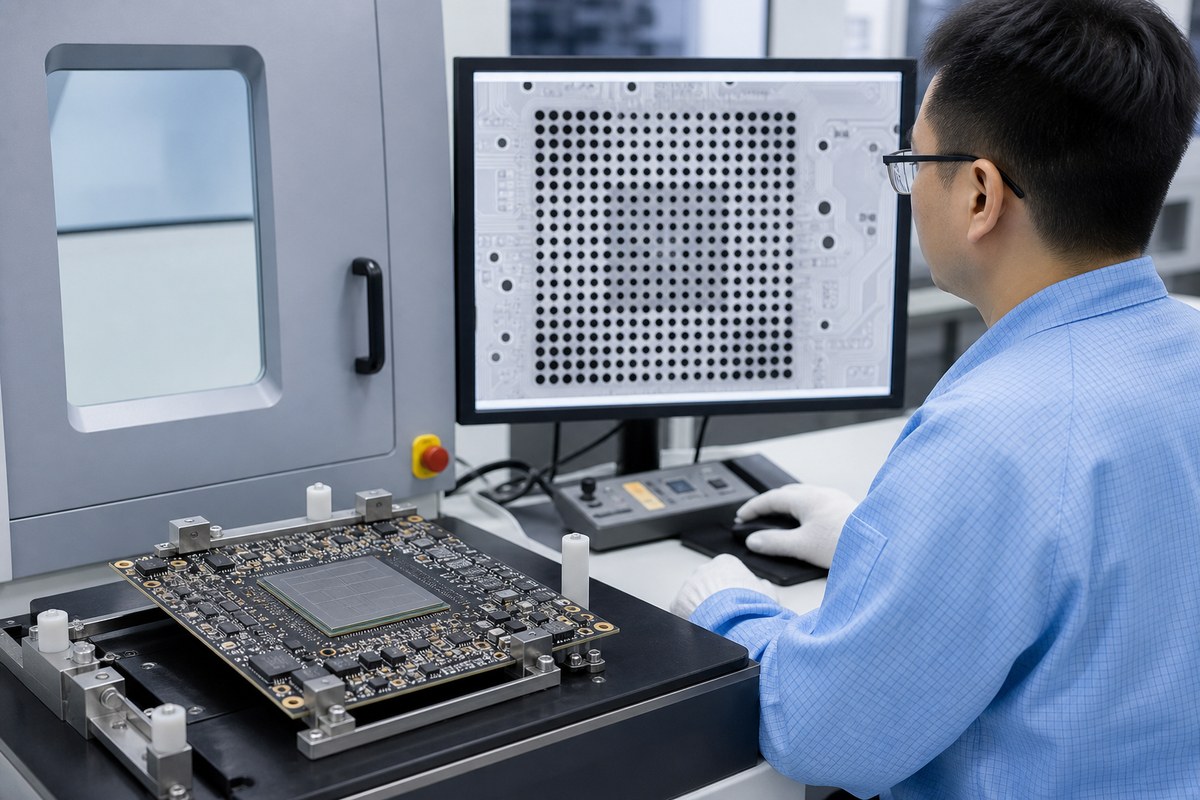
- Hidden solder joints: BGAs and bottom-terminated devices cannot be fully assessed by visual inspection alone.
- Uneven heating: Heavy copper, large ground areas, connectors, and heatsinks can create different heating and cooling rates.
- Paste-volume conflict: Fine-pitch devices and large thermal pads may require different stencil strategies.
- Moisture exposure: Improper storage or handling of moisture-sensitive devices can damage packages during reflow.
- Mechanical loading: Stiffeners, heatsinks, and mounting hardware can stress the assembled board if their sequence or torque is not controlled.
Consider an accelerator card with a large BGA, low-loss multilayer PCB, back-drilled high-speed vias, and high-current power stages. If the stackup changes after electrical approval, or the reflow plan ignores board and package warpage, the prototype may pass continuity testing yet fail under load or temperature cycling.
For this type of project, EBest Circuit can coordinate the approved BOM, component handling, stencil review, placement, reflow, AOI, X-ray, and customer-defined test steps under one revision-controlled build. Programming files, functional limits, fixtures, and final product acceptance requirements should be supplied or approved by the customer.
How Are AI Accelerator PCBs Inspected and Tested?
AI accelerator PCBs are inspected in stages because bare-board defects, placement errors, hidden solder joints, and functional failures require different methods.
Bare PCB inspection
- AOI checks the patterned layers for selected opens, shorts, and image defects.
- Electrical testing checks network continuity and isolation.
- Impedance coupons and TDR verify agreed controlled structures.
- Dimensional or microsection records may be added when specified.
Assembly inspection
- SPI can check solder-paste deposition when included in the inspection plan.
- AOI checks component presence, position, polarity, and visible solder joints.
- X-ray examines hidden BGA and bottom-terminated solder joints.
- First-article records confirm the approved revision and assembly condition.
Electrical and functional testing
- ICT or boundary scan can detect defined assembly and connectivity faults.
- Programming verification confirms that the specified device image was loaded.
- Fixture-based functional tests check customer-defined operating conditions.
- Burn-in or environmental screening is used only when the project specification requires it.
No single result proves the complete product. Before production, the customer and supplier should agree which reports are required, how sampling will work, what constitutes acceptance, and how failures will be handled. This avoids receiving a stack of inspection reports that does not answer the product’s real risks.
How to Choose an AI Accelerator PCB Manufacturer?
Choose an AI accelerator PCB manufacturer by checking whether it can control the complete combination of stackup, materials, HDI features, assembly risks, and quality evidence required by your board.
Ask each candidate to provide:
- A producible stackup with named materials and realistic alternatives.
- DFM feedback on the features most likely to affect yield or reliability.
- A clear plan for impedance control, HDI, back drilling, copper balance, and board flatness where applicable.
- BGA assembly, moisture handling, warpage, reflow, AOI, and X-ray controls.
- Component sourcing and traceability controls for PCBA orders.
- Defined test methods, sampling, acceptance criteria, and report outputs.
- A revision-control process covering quotation, fabrication, assembly, programming, and testing.
EBest Circuit’s advantage is the ability to connect these stages rather than treating the PCB, components, assembly, and inspection as unrelated purchases. One engineering and production path can help reduce stackup mismatches, uncontrolled material substitutions, BOM revision errors, and gaps between assembly risk and inspection evidence.
Send the same controlled data package to each supplier so quotations are comparable. A useful quotation should identify the material system, stackup assumptions, special processes, tooling, inspection, test scope, lead-time conditions, and unresolved questions—not only a headline price.
FAQs About AI Accelerator PCB
What files are needed for an AI accelerator PCB quotation? Provide Gerber or approved fabrication data, a fabrication drawing, drill files, stackup or impedance requirements, dimensions, tolerances, quantity, and schedule. For assembly, also provide the BOM, centroid data, assembly drawings, approved substitutions, programming needs, and test requirements.
Can one supplier handle both AI accelerator PCB fabrication and assembly? Yes, if the supplier has the required fabrication, sourcing, assembly, inspection, and test capabilities. Using one coordinated partner can reduce revision mismatches between the bare PCB and PCBA stages.
How are large BGA solder joints inspected? AOI checks visible placement and surrounding joints, while X-ray is used for hidden BGA connections. Acceptance criteria should be defined for the package, board, and product rather than inferred from an image alone.
Can an alternative low-loss laminate be used? Sometimes, but it should be evaluated for dielectric properties, copper profile, available thicknesses, thermal behavior, process compatibility, lead time, and its effect on the approved impedance and loss model.
What affects AI accelerator PCB prototype cost and lead time? The main drivers include layer count, material availability, HDI and lamination cycles, via filling, back drilling, impedance requirements, board size, copper weight, component availability, assembly complexity, inspection, testing, quantity, and engineering review.
A reliable AI accelerator PCB depends on the stackup, high-speed channels, power delivery, HDI structure, assembly process, and inspection plan working together. EBest Circuit (Best Technology) can support the project from manufacturability review and PCB fabrication through sourcing, BGA assembly, X-ray inspection, and customer-defined testing.
Send your fabrication data, stackup, BOM, and test requirements to sales@bestpcbs.com for a project-specific AI accelerator PCB review and quotation.