





Quick turn PCB boards shorten the path to testable hardware. That speed matters only when the fabrication data are complete, the stackup is manufacturable, components are available and inspection requirements are defined before work starts. For urgent PCB projects, EBest Circuit coordinates design support, prototyping, fabrication, component sourcing and assembly through one technical contact.
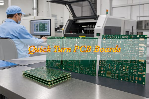
What Are Quick Turn PCB Boards?
Quick turn PCB boards use an expedited production schedule. They are commonly used for prototypes, engineering validation, urgent replacement builds and low-volume product iterations. “Quick turn” is not one universal number: it may describe bare-board fabrication only, fabrication plus assembly, or the entire interval through shipment.
A useful quotation names both the starting and finishing events. Fabrication time normally starts after the files pass engineering review and all commercial questions are closed. Assembly time may start only after the boards, stencil data and approved components are available. Factory time and shipping time belong on separate lines.
How Long Does Quick Turn PCB Manufacturing and Assembly Take?
Bare boards can take 24 hours to 10 working days. Complete turnkey PCB fabrication and assembly commonly needs 7–15 working days. The shortest window applies to small quantities of standard rigid boards with approved data and available materials. Fabrication time starts after engineering questions are closed; assembly time starts after the last required component is available.
| Quick-Turn Order | Typical Factory Time | When the Time Applies |
| 1–2 layer rigid FR-4 bare PCB | 24–48 hours | Small prototype quantity, standard material, standard finish and no unresolved DFM issue |
| 4 layer rigid FR-4 bare PCB | 2–3 working days | Approved standard stackup, conventional through vias and material in stock |
| 6–8 layer rigid multilayer PCB | 3–5 working days | Stackup and impedance structure approved before CAM release |
| 10+ layer, HDI or sequential-lamination PCB | 5–10 working days | Depends on microvia cycles, via filling, special laminate and inspection requirements |
| Simple flex PCB | 3–7 working days | Stock polyimide, simple outline, conventional coverlay and limited layer count |
| Rigid-flex or complex flex PCB | 7–15 working days | Material, stiffener, bend-area, lamination and via structure fully approved |
| Assembly only with all parts consigned | 2–5 working days | Boards, stencil data and complete component kit have arrived and passed incoming check |
| Turnkey PCB fabrication and assembly | 7–15 working days | BOM is approved and every component is available; programming and testing may add time |
These ranges are planning references, not unconditional promises. EBest reports that eligible urgent bare-board orders can be shipped within 24 hours, but the exact commitment must be confirmed after reviewing layer count, materials, quantity, design rules, inspection scope and current capacity. Courier transit and customs clearance are separate from factory time.
What Factors Affect Quick Turn PCB Lead Time and How Can Delays Be Avoided?
The longest unresolved task controls lead time. A rush fee cannot compensate for an unavailable laminate, an obsolete IC or a stackup that has not been approved. The schedule is easier to protect when every risk has a named action, responsible contact and deadline.
- Layer count and lamination cycles: every multilayer pressing cycle, blind/buried-via sequence or HDI buildup adds fixed process time. Avoid delay by approving a manufacturable stackup before order release.
- Material availability: special high-frequency laminates, unusual thicknesses, heavy copper and uncommon solder-mask or finish combinations may require procurement. Confirm stock or approve an electrically suitable alternative first.
- Design-rule exceptions: fine traces, small annular rings, high aspect ratios, tight solder-mask dams and copper-to-edge conflicts trigger engineering questions. Run DFM before starting the clock.
- Controlled impedance: the fabricator may need to adjust trace width for the selected laminate and finished copper. Provide target impedance, tolerance and reference layers, then authorize one approver to sign off quickly.
- Component shortages: one unavailable connector or programmed IC can stop an entire PCBA. Lock manufacturer part numbers, identify acceptable alternates and review lifecycle status before ordering.
- Revision control: mismatched Gerber, drill, BOM and centroid revisions cause holds or wrong builds. Put the same revision and release date on every file and withdraw superseded packages.
- Test preparation: functional tests can be delayed by missing firmware, cables, fixtures or acceptance limits. Release test assets with the production package, not after assembly.
- Approval response: unanswered engineering questions leave material and machines idle. Nominate a technical contact who can approve stackup, substitutes and deviations within the same working day.
A practical schedule lists five milestones: data approval, material/component readiness, bare-board completion, assembly/test completion and shipment. With those dates visible, a delay can be traced to engineering, procurement, production or logistics.
What PCB Types and Technologies Support Quick Turn Production?
Many PCB technologies can use quick-turn production. EBest’s product range covers the technologies below; each urgent build still needs material and construction review.
| PCB Type or Technology | Suitable Quick-Turn Work | What Must Be Confirmed |
| Single-sided and 2–8 layer FR-4 | Prototype, design revision, pilot build and replacement board | Standard stackup, copper weight, finish and drill rules |
| Multilayer and controlled-impedance PCB | High-speed controller, communication and computing prototypes | Layer order, dielectric thickness, impedance targets, coupons and tolerance |
| HDI and extra-thin PCB | Dense portable, sensor and compact control electronics | Microvia structure, sequential lamination, via fill, fine-line capability and handling |
| Flex and semi rigid-flex PCB | Cable replacement, moving interconnect and space-limited prototypes | Polyimide, coverlay, stiffeners, bend zones and dimensional tooling |
| Rigid-flex PCB | Integrated three-dimensional interconnect prototypes | Rigid/flex transition, no-flow material, coverlay, via placement and lamination sequence |
| Metal-core, busbar and heavy-copper PCB | LED, power conversion, motor control and high-current evaluation | Base metal, dielectric system, copper thickness, thermal path and profiling method |
| Ceramic PCB | Power module, high-temperature and compact thermal prototypes | Alumina/AlN substrate, metallization, copper structure and available panel format |
| RF, high-frequency and high-speed PCB | RF front end, antenna feed, radar and high-speed link evaluation | Specified laminate, Dk/Df basis, surface finish, impedance and RF test coupon |
| High-Tg and impedance-control PCB | Thermally demanding or signal-sensitive industrial builds | Exact laminate grade, Tg requirement, stackup and measurable acceptance criteria |
For the fastest route, provide both the preferred construction and the electrical or mechanical requirement behind it. Compare the design with the supplier’s verified PCB manufacturing capability. Engineering can then determine whether an in-stock material or standard build achieves the same function without introducing a new qualification risk.
What Files Are Required for a Quick Turn PCB Online or Instant Quote?
Reliable quotes require a complete build package. Use one ZIP file with a clear revision name, remove obsolete outputs and include a short read-me that identifies quantity, requested factory date and the authorized technical contact.
- Fabrication image data: a complete PCB Gerber file package in RS-274X, ODB++ or another agreed intelligent format covering every copper, solder-mask, legend and paste layer.
- NC drill and route data: separate plated and non-plated drills where applicable, slots, countersinks, depth-controlled features and the final board outline.
- Fabrication drawing: finished dimensions, tolerances, layer order, material, finished thickness, copper weight, surface finish, solder-mask/legend requirements, via treatment and special notes.
- Stackup and impedance table: signal/reference layers, target ohms, tolerance, trace type and any differential pair requirement. State whether the fabricator may adjust geometry.
- Panel requirement: individual board or array, rail width, breakaway method, tooling holes, fiducials and any assembly-panel constraints.
- Assembly BOM: reference designators, quantity, value, package, manufacturer, exact MPN, approved alternative and do-not-substitute status.
- Centroid/pick-and-place file: X/Y position, rotation, board side and reference designator using the same origin and revision as the assembly drawing.
- Assembly drawings: component outlines, polarity, pin 1, no-fit/DNP parts, selective soldering, hardware, cable and mechanical instructions.
- Programming and test package: firmware version, programming steps, connectors, power limits, fixture/cable definition, test sequence, pass/fail limits and required records.
- Commercial inputs: bare-board and assembled quantities, acceptable overage, consigned parts list, delivery destination, shipping terms and requested date.
Before uploading, view the final package and check layer alignment, mirrored bottom data, drill registration, outline closure, polarity and BOM-to-centroid consistency. Name every file with the same project and revision identifier. If the quote tool cannot represent a special requirement, write it in the fabrication drawing and request manual engineering review rather than selecting the closest option.
How Does the Quick Turn PCB Manufacturing Process Work?
Quick-turn builds still use the complete fabrication route. Physical operations such as lamination, plating, curing and testing cannot simply be skipped or shortened below their controlled process window.
- Order and revision intake: confirm quantity, delivery target, fabrication format, drawing, stackup and revision. CAM should stop if the drill, outline or drawing conflicts with the image data.
- DFM and stackup review: check trace/space, annular ring, drill-to-copper distance, hole aspect ratio, copper balance, solder-mask clearance, controlled impedance and panel utilization. Return one consolidated engineering-question list.
- CAM tooling and panelization: generate production panels, tooling holes, fiducials, test coupons, drill programs and rout/V-score paths. Apply controlled compensation for etching, plating and finished dimensions.
- Material cutting and preparation: allocate the approved laminate, prepreg and copper foil; cut panels and prepare copper surfaces. Material identity must match the traveler before imaging.
- Inner-layer imaging and etching: transfer internal circuitry, develop and etch unwanted copper. AOI compares the finished inner layers with CAM data before they become inaccessible inside the multilayer structure.
- Oxide treatment and lamination: prepare inner-layer copper, stack cores and prepregs in the correct order, then press under the qualified heat and pressure cycle. Multilayer registration is checked after lamination.
- Mechanical or laser drilling: drill through holes, blind/buried vias, microvias, slots and tooling features according to the released program. Deburr and desmear holes so the plating can form a reliable interconnect.
- Electroless copper and electroplating: deposit conductive copper in the hole walls, then build the specified copper thickness. Plating uniformity, hole-wall condition and copper thickness are process-control points.
- Outer-layer imaging and etching: form the external circuitry and inspect it for opens, shorts, under-etch, over-etch and registration defects. Controlled-impedance geometry must remain within the approved build.
- Solder mask and legend: clean the panel, apply and image solder mask, cure it, then print the approved component legend. Pads, fine-pitch openings and solder-mask dams receive visual or automated inspection.
- Surface finish: apply the ordered finish, such as ENIG, HASL or another approved option. The finish must protect exposed copper and meet the assembly and shelf-life requirement.
- Profiling and final dimensions: rout, score or punch the panel; inspect board outline, cutouts, slots, bevels and panel breakaway features against the drawing.
- Electrical and final inspection: test continuity and isolation, inspect appearance and dimensions, verify impedance when specified and review the lot against the agreed acceptance requirements.
- Cleaning, packing and release: clean and dry boards, vacuum or moisture-protect them when required, label the correct revision and release shipment only after quality records are complete.
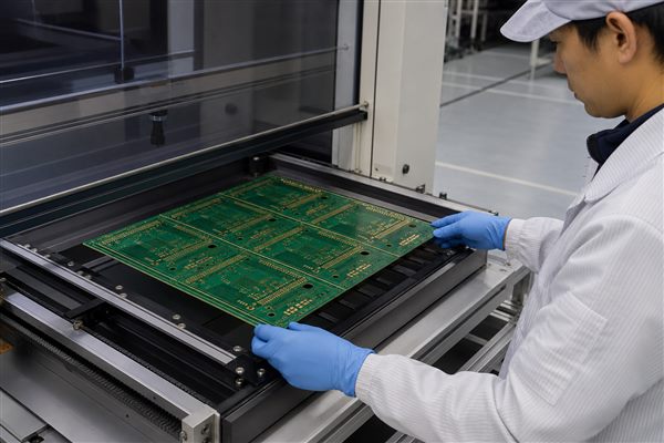
What Is Quick Turn PCB Assembly and What Does Turnkey PCBA Include?
Quick-turn PCB assembly prioritizes population and inspection. A full turnkey scope may include BOM review, approved sourcing, incoming control, stencil preparation, solder-paste printing, SMT placement, reflow, through-hole insertion, cleaning, visual inspection, AOI, X-ray where suitable, programming and agreed testing.
Clarify inclusions before comparing quotations. Some offers cover labor only; others include fabrication, components, stencil, tooling, inspection, programming, test and packaging. Component availability often controls the true schedule, so the BOM should identify exact manufacturer part numbers and whether alternates require written approval.
How Is Quality Controlled During Fast Turn PCB Manufacturing and Assembly?
Quality control follows the complete production route. Expedited scheduling should remove idle queue time, not inspection points. The drawing and purchase order must define the acceptance class, critical dimensions, test scope and required records before fabrication starts.
- Pre-production data control: compare Gerber/ODB++, drill, drawing, stackup, BOM and centroid revisions; document every approved engineering change.
- Incoming material control: verify laminate, copper foil, prepreg, solder mask, surface-finish chemistry and sourced components against the approved order.
- Inner-layer AOI: detect opens, shorts, nicks, residual copper and registration errors before lamination hides the circuitry.
- Drilling and plating control: monitor drill condition, hole location, desmear, plated-hole copper and cross-section quality where the order requires it.
- Outer-layer and solder-mask inspection: check conductor geometry, pad openings, solder-mask dams, legend polarity marks and surface-finish coverage.
- Bare-board electrical test: verify continuity and isolation using flying probe or fixture testing so open and short circuits do not reach assembly.
- Impedance verification: measure the agreed coupon or test structure and retain the result when controlled impedance is part of acceptance.
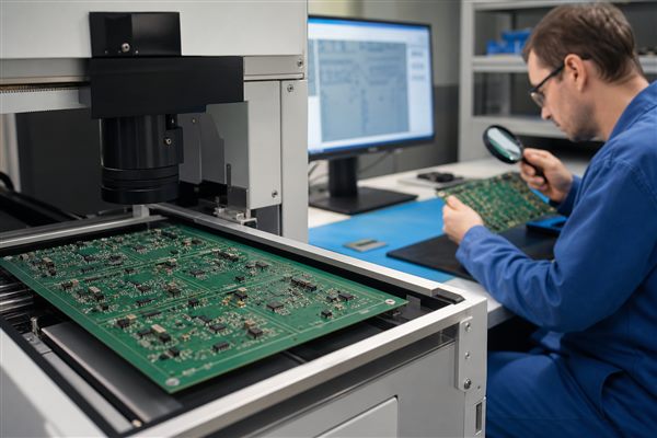
- Solder-paste inspection: check paste volume, area, height and alignment before placement when package density or process risk justifies SPI.
- First-article assembly: verify polarity, orientation, programmed part identity, hardware and workmanship before releasing the remaining lot.
- Post-reflow AOI: inspect placement, polarity, missing parts, tombstoning, solder bridges and visible solder-joint conditions.
- X-ray inspection: examine hidden BGA, QFN, bottom-terminated or other inaccessible joints when the package and acceptance plan require it.
- Programming and functional test: load the controlled firmware version, apply defined power limits and confirm the specified inputs, outputs and communication functions.
- Final documentation: ship the inspection, electrical, impedance, programming or functional-test records explicitly required by the order.
What Affects the Cost of Quick Turn PCB vs Standard PCB Production?
Reserved capacity creates the basic quick-turn premium. The final difference is driven by both the rush level and the technical work required. A standard two-layer board made from stocked material has a smaller premium than a multilayer HDI build that needs sequential lamination, filled microvias and special testing.
| Cost Driver | Quick-Turn Cost Effect | How to Control It |
| 24-hour or weekend priority | Requires reserved machines, priority CAM, separate handling or overtime | Use the fastest tier only for boards that control the project schedule |
| Very small quantity | Tooling, CAM, setup and inspection costs are divided across fewer boards | Order enough units for build, rework, test and one backup iteration |
| Layer count and lamination | More cores, prepregs, pressing cycles and registration checks increase labor and machine time | Use an approved standard stackup when electrical performance permits |
| HDI, blind/buried vias and via fill | Laser drilling, sequential buildup, filling, planarization and added inspection create separate operations | Use the minimum via complexity required by routing and package escape |
| Special laminate | High-frequency, ceramic, flex or uncommon high-Tg material may need dedicated procurement and setup | Confirm stock and approve suitable alternates before the rush clock starts |
| Heavy copper or unusual thickness | Changes etching, plating, drilling, lamination and profiling conditions | Define the actual current, thermal and mechanical requirement instead of over-specifying |
| Tight design rules | Fine lines, small holes, tight mask dams and narrow tolerances reduce process margin and may need extra control | Run DFM and relax noncritical features before release |
| Surface finish | Uncommon or multi-finish requirements can add chemistry, handling and queue time | Select the finish from assembly, contact and shelf-life needs |
| Component availability | Spot buys, split shipments, substitutes and shortages can dominate turnkey PCBA cost | Lock the BOM early and approve alternates by manufacturer part number |
| Assembly complexity | Fine-pitch, BGA/QFN, double-sided SMT, THT, press-fit, hand soldering and rework require different setups | Provide complete assembly data and identify critical packages during quoting |
| Test and documentation | Fixtures, programming, X-ray, functional tests, microsections and reports add engineering time | Specify the evidence needed for product risk and acceptance |
| Express freight | Fast courier and split shipment may cost more than the board build | Separate factory completion, shipment and arrival dates before comparing quotes |
Compare quick-turn and standard quotations using the same revision, quantity, test scope, component source, delivery destination and shipping terms. The cheapest practical option is often to expedite the first engineering lot, close design issues quickly and move the approved revision to a standard production schedule.
Where Are Quick Turn PCB Boards Commonly Used?
Quick-turn boards support time-sensitive hardware needs. Typical applications include:
- Engineering prototypes: turn a new schematic and layout into hardware for power-up, interface, thermal and firmware validation.
- Design respins: correct a footprint, routing, EMC, power or mechanical problem and test the revised board before the next review gate.
- Pilot and NPI builds: verify panelization, assembly instructions, programming, test coverage and production documentation before volume release.
- Medical electronics development: build controlled engineering samples for diagnostic, monitoring or laboratory equipment while maintaining the applicable traceability and approval requirements.
- Aerospace electronics development: produce prototype control, communication or power hardware with explicit material, change-control and acceptance records.
- Industrial equipment repair: replace an unavailable controller, sensor interface, motor-control or power board to reduce machine downtime.
- Automotive engineering samples: evaluate control, lighting, power-conversion or sensor electronics before formal qualification and production approval.
- RF and communication prototypes: test antenna feeds, RF front ends, impedance structures and high-speed interfaces on physical hardware.
- Test fixtures and adapters: create bed-of-nails interfaces, programming boards, breakout boards and production-line diagnostic tools.
- Demonstration and evaluation units: supply working hardware for investor, product or internal design reviews without waiting for a mass-production lot.
- Bridge production: cover a short demand window while the approved volume-production route, tooling or supply chain is being prepared.
For regulated or safety-related products, quick-turn production accelerates hardware availability but does not replace qualification, validation or required product approval.
How to Choose a Reliable Quick Turn PCB Manufacturer and Assembly Supplier?
Reliable suppliers provide a build-specific plan. Evaluate the supplier point by point:
- Confirm the schedule definition: require the quote to state when the clock starts and whether the commitment means fabrication complete, assembly complete, shipped or delivered.
- Request pre-order engineering review: the supplier should check stackup, design rules, drill structure, panelization, BOM and test needs before promising the date.
- Verify technology fit: confirm the exact layer count, material, copper thickness, HDI/flex/rigid-flex structure, impedance and finish—not merely a broad capability category.
- Check material and component stock: an urgent production slot has little value if laminate or one critical IC is unavailable.
- Control substitutions: require written approval before changing manufacturer, MPN, package, rating or lifecycle status.
- Review the quality route: identify bare-board electrical test, AOI, impedance verification, SPI, X-ray, programming and functional testing included in the quote.
- Define communication ownership: one project contact should coordinate CAM, sourcing, assembly, quality and logistics and issue one consolidated question list.
- Ask for order-specific records: agree which inspection, electrical, impedance, programming or functional-test records will ship with the order.
- Check prototype-to-production control: the supplier should preserve the approved stackup, BOM, assembly instructions and deviations for repeat production.
- Compare total delivered risk: include tooling, components, testing, rework policy, express freight and the cost of a missed project milestone—not only the bare-board price.
A qualified custom PCB supplier should summarize the released revision, remaining assumptions, confirmed material/components, inspection plan and committed ship date in one response. If these items are unclear, the advertised turnaround time is not yet a dependable schedule.
What Quick Turn PCB Manufacturing and Assembly Services Can We Provide?
EBest provides one-stop PCB and PCBA support. As a PCB prototype manufacturer, EBest can connect early design validation with sourcing, assembly and later production. Available services include:
- PCB design support: review design inputs and help prepare a manufacturable package before urgent production release.
- PCB prototypes: support engineering samples and low-volume validation builds, including eligible expedited bare-board orders.
- Mass production: transfer an approved prototype revision into repeat or volume manufacturing with controlled data continuity.
- Component sourcing: source BOM items, identify availability risks and coordinate approved alternatives with assembly planning.
- PCB assembly: coordinate SMT, through-hole or mixed assembly according to the released BOM, placement data and drawings.
- Standard FR-4 and multilayer PCB: manufacture single-sided, conventional rigid and multilayer constructions for general electronics.
- Metal-core and busbar PCB: support thermal and high-current applications that need an aluminum/metal base or heavy current path.
- Ceramic PCB: support compact power, thermal and high-temperature applications requiring a ceramic substrate.
- Flexible and rigid-flex PCB: build bendable or integrated rigid/flex interconnects for space-constrained products.
- RF, high-frequency and high-speed PCB: support material and stackup requirements for signal-sensitive designs.
- High-Tg, heavy-copper and impedance-control PCB: support thermal, current-carrying and controlled-transmission requirements.
- HDI and extra-thin PCB: support dense interconnect and thickness-constrained electronics after process feasibility review.
- Engineering and quotation support: review files, identify the quick-turn critical path and provide an order-specific quotation.
For the fastest review, send fabrication data, quantity and requested ship date. For assembly, also send the BOM, centroid file, assembly drawing, firmware and test requirements.
Why Choose EBest Circuit as Your Quick Turn PCB Manufacturer?
Integrated services reduce supplier handoff time. The practical advantages are:
- One accountable project route: PCB design, prototype fabrication, component sourcing and assembly can be coordinated through one engineering path, reducing handoff delays and conflicting revisions.
- Early manufacturability decisions: stackup, drill structure, copper, material, finish and panel requirements can be reviewed before the rush schedule is committed, reducing the risk of a production hold.
- Broad construction coverage: FR-4, multilayer, metal-core, ceramic, flex, rigid-flex, RF, high-frequency, high-Tg, heavy-copper, HDI, extra-thin, busbar, high-speed and impedance-controlled options allow the construction to be matched to the application rather than forced into one standard board type.
- BOM and assembly coordination: component availability, alternates, placement data and test requirements can be checked together, preventing the bare PCB from finishing while assembly waits for unresolved parts.
- Expedited capability with feasibility control: eligible urgent bare boards may ship within 24 hours after engineering and schedule review; complex builds receive an order-specific commitment instead of an unrealistic blanket promise.
- Capacity for mixed project needs: EBest reports monthly PCB capability of about 260,000 square feet and more than 1,000 different board builds, supporting a mix of prototype and production work. Availability still needs confirmation for each urgent order.
- Quality systems relevant to demanding markets: EBest reports IATF 16949, ISO 9001:2015, ISO 13485:2016, AS9100D, REACH, RoHS and UL credentials. The current certificate or listing relevant to the product and order should be confirmed before release.
- Prototype-to-volume continuity: the approved stackup, fabrication package, BOM, assembly notes and deviations can become the controlled baseline for repeat production, reducing requalification and communication work.
The real advantage is controlled execution, not a shorter date on paper. Released design data move through one traceable route to boards ready for validation and the next production decision.
Quick Turn Multilayer PCB Manufacturing and Assembly Case Study
This case follows an urgent multilayer controller PCBA. The project requires one controlled revision for fabrication, sourcing, assembly, programming and functional verification.
Project Background: A product-development team needs assembled controller boards for bench testing before its mechanical and firmware review. The board includes a multilayer power/ground structure, controlled-impedance signals, fine-pitch SMT devices, connectors and several programmed components. A late layout revision has changed two footprints and the board outline, so fabrication and assembly must use the same release.
Project Requirements: The released package includes Gerber/ODB++, plated and non-plated NC drill files, stackup, impedance table, fabrication drawing, BOM, centroid data, assembly drawings and firmware. The BOM marks exact manufacturer part numbers, do-not-substitute devices and approved alternates. The test package defines input-voltage limits, connector pinout, programming version and the outputs that must be checked.
Our Solution: EBest engineering first compares the outline, drill, copper, BOM and centroid revisions and returns one consolidated question list. CAM reviews annular rings, copper-to-edge clearance, solder-mask openings, panel rails and impedance geometry. Sourcing confirms the critical ICs and connectors before the assembly schedule is released. The approved array includes tooling holes and fiducials for SMT. Inner-layer AOI, bare-board electrical test and impedance verification are assigned before fabrication; first-article polarity, paste, placement and programmed-part checks are assigned before the remaining assemblies proceed.
Output Results: The project output is a traceable package: approved engineering responses, a frozen fabrication and assembly revision, fabricated multilayer boards, assembled controller units, and the electrical, inspection, programming or functional-test records specified by the order. The approved package also establishes a controlled baseline for the next design iteration or production quotation.
FAQs About Quick Turn PCB Boards
Q1: Which surface finish is practical for an urgent prototype?
A1: Choose the finish from assembly and contact needs. ENIG is often selected for flat pads and fine-pitch assembly, while HASL may suit less demanding standard boards. Availability, shelf life, wire bonding, edge contacts and the component package must be reviewed before selecting a finish only for speed.
Q2: How many boards should I order for the first prototype run?
A2: Include units for testing, rework and one backup build. Ordering only the exact number needed for a demonstration creates risk if one board is used for destructive analysis or damaged during bring-up. The right quantity depends on test coverage, assembly yield risk and how quickly another revision can be released.
Q3: Should I panelize the PCB before sending it to the manufacturer?
A3: Send the individual design unless the assembly array is already controlled. The manufacturer can normally create a fabrication panel, while the assembler may need rails, fiducials and tooling holes. If you supply an array, clearly define breakaway method, rail width, fiducials and acceptable rotated boards.
Q4: Can the fabricator change trace width for controlled impedance?
A4: Only with documented authorization. Finished copper and actual dielectric thickness may require a different trace width from the nominal layout. State the impedance target and tolerance, identify reference layers and authorize the fabricator to propose geometry changes for approval before imaging.
Q5: Are alternative laminate brands acceptable on a prototype?
A5: An alternative is acceptable only when the required properties still match. Review Tg, Dk, Df, thickness, copper, thermal behavior, flammability and qualification needs. For signal-sensitive or regulated designs, changing material may require engineering approval or new validation even if it shortens procurement time.
Q6: Does a quick-turn assembly order need a new stencil?
A6: Most SMT assemblies require a stencil matched to the released paste data. Apertures may need adjustment for fine-pitch, thermal pads, small passives or mixed component sizes. Reusing an old stencil is safe only when the PCB revision, paste openings, thickness and process requirements remain compatible.
Q7: How should consigned components be packed and identified?
A7: Preserve traceability and moisture protection. Label each package with project, revision, MPN, quantity and reference designators. Keep moisture-sensitive parts sealed with the required desiccant and indicator, provide MSL information, and separate programmed or project-specific devices to prevent uncontrolled substitution.
Q8: Can functional testing be added without a custom fixture?
A8: Simple bench testing may be possible with accessible connectors and test points. Provide the power supply limits, cable pinout, firmware, test sequence and pass/fail criteria. Higher volume or complex coverage may require a fixture, which should be included in the schedule and quotation.
Q9: What packaging should be specified for assembled boards?
A9: Packaging should protect ESD-sensitive parts and exposed mechanical features. Common controls include ESD-safe bags, moisture protection, trays, foam or blister packaging for tall components, and labels showing part number and revision. Identify connectors, displays or protruding hardware that cannot carry stacking load.
Q10: Can the same prototype data be reused for mass production?
A10: Yes, after the prototype changes are incorporated into a controlled release. Record approved stackup adjustments, component substitutions, assembly notes, test limits and deviations. Issue a new production revision rather than relying on email history, then confirm panel efficiency, tooling and volume test strategy.
Conclusion
Successful quick-turn builds start with complete inputs. When fabrication, sourcing, assembly and testing work from the same released revision, your team receives usable hardware sooner and avoids losing the saved time to clarification, rework or uncontrolled changes.
Do you have a prototype deadline, an urgent multilayer board or a turnkey PCBA waiting for a realistic schedule? Send EBest Circuit your Gerber or ODB++ files, drill data, stackup, quantity and required ship date. For assembly, include the BOM, centroid file, drawings and test requirements. Our engineering team will review the critical path, identify any missing information and prepare an order-specific manufacturing and assembly quotation.
Send your project package to sales@bestpcbs.com today and tell us the date your boards must ship. We will evaluate the fastest practical route for your design and help you move from released files to testable hardware with clear responsibilities and controlled quality.
You may also like





Tags: PCB Assembly, pcb manufacturing, pcb prototype, Quick Turn PCB