






Telecom PCB manufacturing services cover the fabrication, assembly, inspection and testing decisions needed for communication equipment boards, especially when RF behavior, signal integrity, material choice, shielding, thermal load or production repeatability matters. The right supplier should help the buyer review the board as an engineered communication product, not only quote a generic PCB.
This guide explains how to compare telecom PCB suppliers, what the current supplier comparison landscape show, which technical requirements should be clarified, and what files to send for a useful RFQ.
Telecom PCB Manufacturing Services at a Glance
A telecom PCB service should connect bare board fabrication, DFM review, assembly planning, RF-related checks, testing expectations and quote assumptions. The exact requirement depends on whether the board is a base station module, router board, antenna interface, IoT gateway, fiber equipment board, power board or control PCB.
| Area | What to confirm | Why it matters |
|---|---|---|
| Electrical behavior | Controlled impedance, RF paths, return paths and signal integrity needs | Telecom boards can fail even when the bare board passes simple continuity tests. |
| Materials | FR-4, high-frequency material, hybrid stackup or project-specific laminate | Material choice affects loss, stability, cost and manufacturability. |
| Assembly | BOM, CPL, shielding, connectors, polarity and inspection access | RF modules, connectors and shielding parts can drive assembly risk. |
| Testing | Electrical test, AOI, X-ray if needed, functional or RF test responsibility | The buyer must know what the supplier can verify before shipment. |
Is Your Telecom PCB Project Exposed to RF, Thermal or Assembly Risk?
Telecom PCB buyers need supplier review that connects RF material, stackup, impedance, thermal load, assembly and testing.
| Customer Pain Point | Project Risk | How bestpcbs Helps |
|---|---|---|
| RF material and stackup are not reviewed together | Signal behavior may not match the application requirement | bestpcbs asks for frequency range, stackup notes, material expectations and impedance targets before production. |
| Thermal and power requirements are unclear | The board may work in prototype but struggle in operating conditions | bestpcbs reviews copper, board structure, component placement and thermal notes during DFM review. |
| Assembly data is separated from fabrication data | Connectors, shields or RF components may create handling and inspection risks | bestpcbs checks BOM, CPL, assembly drawings and polarity notes when PCBA is required. |
| Test requirements are not stated early | The buyer may not get the right verification for telecom use | bestpcbs confirms electrical, impedance or customer-defined tests during RFQ preparation. |
Telecom PCB Buyer Priorities Before Supplier Selection
Telecom PCB buyers should confirm RF behavior, stackup, material needs, impedance control, thermal load, assembly requirements and test expectations before selecting a supplier. Communication equipment can be sensitive to material and layout assumptions.
Provide frequency range, impedance targets, stackup notes, RF layout constraints, BOM, CPL and testing requirements early. A supplier review before production helps reduce delays caused by missing material, assembly or inspection details.
What Makes Telecom PCBs Different?
Telecom PCBs are different when the board carries RF signals, high-speed data, stable clocking, dense connectors, shielding, thermal load or long production life requirements. Not every telecom board is high-frequency, but every telecom project should identify which sections are electrically sensitive.
A simple control board inside communication equipment may use standard PCB rules. A board with antennas, RF front ends, filters, high-speed interfaces or impedance-controlled lines needs closer review. For RF-specific buying questions, the RF PCB manufacturer RFQ guide is a useful supporting reference.
Materials and Stackup for Telecom PCB Projects
Material and stackup should be selected after the signal behavior, thermal load, layer count, impedance needs and assembly process are understood. Standard FR-4 may be appropriate for many control and power areas, while RF or high-speed sections may need a different laminate or hybrid construction.
Buyers should send the target stackup, copper weight, impedance requirements, operating frequency if relevant, board thickness, surface finish and any thermal notes. Exact material capability and special process limits must be confirmed from the latest project data before order release.
RF, Impedance and Signal Integrity Checks
RF and impedance requirements should be stated in the fabrication notes instead of left for the supplier to infer from the Gerber files. Missing impedance targets, reference planes, material assumptions or test methods can create quote changes and production uncertainty.
- State controlled impedance values and tolerance requirements if applicable.
- Provide stackup targets and dielectric material expectations.
- Identify RF paths, antenna areas, ground references and shielding zones.
- Clarify whether the supplier is responsible for impedance coupon testing.
- Separate ordinary digital/control areas from RF-sensitive sections.
Telecom PCB Assembly and Component Sourcing
Telecom PCB assembly should be planned with connectors, shielding, RF modules, fine-pitch components, thermal parts and component availability in mind. A bare PCB quote does not answer whether the final board can be assembled cleanly.
If the project needs mounted components, prepare BOM, CPL, assembly drawing, polarity notes, approved substitutes and any testing instructions. The PCBA service is the right internal path when fabrication, assembly and sourcing need to be reviewed together.
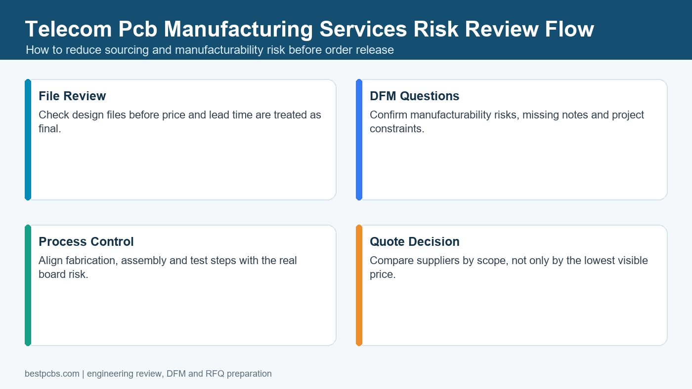
DFM Review Before Telecom PCB Production
DFM review should catch manufacturability risks before the telecom board is quoted as a production job. This includes drill-to-copper clearance, solder mask openings, fine-pitch pads, via design, copper balance, controlled impedance notes, panelization and assembly access.
For production-oriented layouts, compare the board against a PCB design and manufacturing DFM guide before release. If RF or high-speed rules are unclear, label them as targets and ask the supplier to confirm what can be manufactured and tested.
Testing and Inspection for Telecom PCBs
Testing should be defined before the order because telecom boards may need more than a standard bare-board electrical test. A supplier can verify open/short conditions, visual quality and assembly defects, but RF performance or functional behavior may need buyer-supplied fixtures and acceptance rules.
| Test or inspection | What it checks | Buyer input needed |
|---|---|---|
| Electrical test | Bare board opens and shorts | Gerber, netlist and test expectations |
| AOI / visual inspection | Soldering, placement and visible defects | Assembly files, polarity and acceptance criteria |
| Impedance test | Controlled impedance coupon or trace behavior | Target values, tolerance and stackup |
| Functional or RF test | Board-level communication or signal performance | Fixture, firmware, procedure and pass/fail limits |
How to Compare Telecom PCB Suppliers
Compare suppliers by whether they can discuss the actual telecom risk in the board, not only by whether they list PCB manufacturing services. A good supplier should ask about stackup, impedance, materials, assembly files, test method and delivery requirements.
- Can the supplier review RF or impedance notes before quote approval?
- Can they support both PCB fabrication and assembly if required?
- Do they identify special materials or processes that need confirmation?
- Do they explain what testing is included and what requires buyer fixtures?
- Can they quote prototype, low-volume and repeat production needs separately?
What Determines Telecom PCB Manufacturing Cost?
Telecom PCB cost is shaped by material, layer count, impedance control, board size, copper, finish, connector complexity, assembly method, testing, quantity and delivery expectations. A lower quote may be valid for a simple control board but incomplete for an RF or high-speed communication board.
For cost planning, compare telecom requirements with the custom PCB cost guide, then ask suppliers to quote the same stackup, finish, testing and assembly scope.
RFQ Checklist for Telecom PCB Manufacturing Services
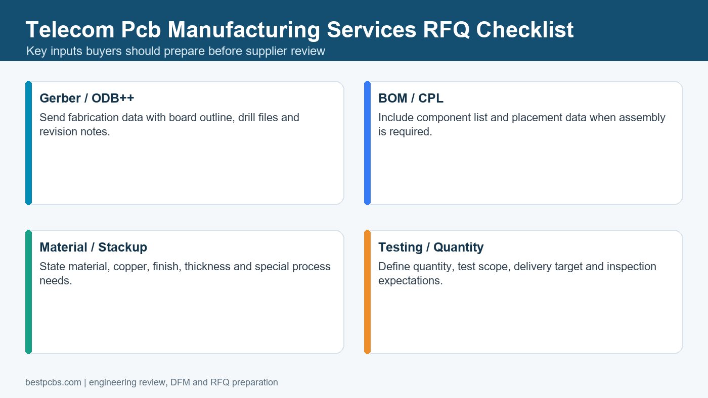
A telecom PCB RFQ should include enough detail for the supplier to identify fabrication, assembly and testing risk before committing to price and lead time. Short requests such as “telecom PCB quote” usually lead to follow-up questions.
- Gerber or ODB++ files, drill data and fabrication drawing.
- Layer count, stackup, material, copper, thickness and surface finish.
- Controlled impedance values, RF notes or high-speed constraints if applicable.
- BOM, CPL, assembly drawing, polarity notes and substitute rules for PCBA.
- Quantity, prototype or production stage, target lead time and delivery destination.
- Electrical test, impedance test, functional test or RF test expectations.
Frequently Asked Questions About Telecom PCB Manufacturing
Are all telecom PCBs high-frequency PCBs?
No. Some telecom boards are power, control or interface boards using standard materials. Others include RF or high-speed sections that need special stackup, material and impedance review.
Can one supplier handle telecom PCB fabrication and assembly?
Yes, if the supplier supports both PCB manufacturing and PCBA. A combined review can reduce handoff mistakes between Gerber files, BOM, CPL, assembly notes and testing requirements.
What should I send for a telecom PCB quote?
Send Gerber or ODB++, drill files, stackup, material, impedance notes, finish, quantity and delivery target. For assembly, also send BOM, CPL, drawings, polarity notes and test requirements.
How do I avoid quality problems in telecom PCB sourcing?
Define the sensitive circuit areas, state material and test assumptions, request DFM review, and confirm what the supplier can actually verify before shipment.
Final RFQ Recommendation
Before choosing telecom PCB manufacturing services, identify whether the board is mainly standard fabrication, RF/high-frequency, high-speed, assembly-heavy or test-heavy. The supplier can quote more accurately when the technical risk is visible.
For a telecom PCB fabrication or assembly quote, send your Gerber or ODB++ files, drill data, stackup, impedance notes, BOM, CPL, assembly drawing, quantity, material expectations, surface finish, testing requirements and target lead time to sales@bestpcbs.com. The Best Technology / bestpcbs team can review the project files and confirm what needs project-specific checking before production.
You may also like


Tags: PCB Assembly, RF PCB, Telecom PCB