

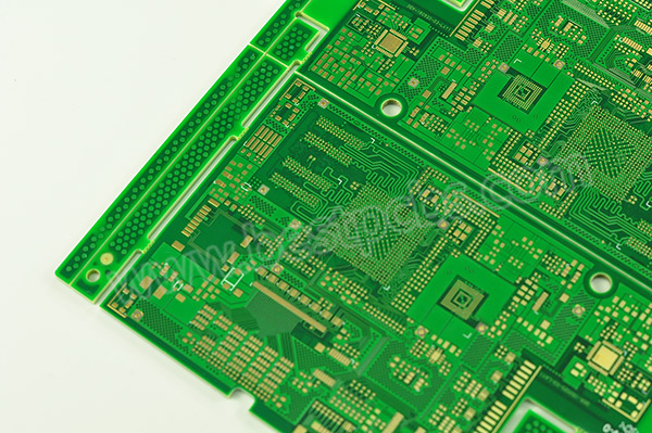
An HDI RF Board is a sophisticated printed circuit board that merges High-Density Interconnect technology with specialized materials and design rules to excel in radio frequency applications. Pushing the limits of modern wireless, radar, and sensing systems demands circuits that are faster, smaller, and more reliable than ever. This article provides a comprehensive guide to understanding HDI RF boards, their advantages for high-frequency designs, key structural elements, cost considerations, comparisons with other substrates, and guidance on selecting a reliable HDI PCB manufacturer.
Are your current PCB solutions holding back your next-generation RF design? You might be facing these common challenges:
- Signal Degradation at High Frequencies: Standard PCB constructions struggle with significant signal loss, crosstalk, and impedance discontinuities, crippling the performance of sensitive RF and microwave circuits.
- Size and Weight Constraints: Achieving complex functionality often means larger, multilayer boards that contradict the miniaturization goals of modern portable and aerospace electronics.
- Thermal Management Headaches: Dense component placement and high-power RF sections generate concentrated heat that standard boards cannot effectively dissipate, leading to reliability risks.
- Prototyping and Yield Frustrations: Complex RF designs often require multiple expensive prototype iterations, and manufacturing defects in fine features can lead to poor yield and project delays.
- Supply Chain and Expertise Gaps: Finding a manufacturer with both advanced HDI technology in PCB fabrication and deep RF/microwave design support is difficult, leading to communication breakdowns and suboptimal results.
The solution lies in partnering with a specialist who masters the fusion of HDI fabrication and RF principles. At BEST Technology, we engineer Premium HDI RF Boards specifically to overcome these hurdles.
- Superior Signal Integrity: We utilize advanced HDI layer stacking, low-loss materials, and precise impedance control to ensure clean, high-fidelity signal transmission for your RF and microwave circuit boards.
- Enabled Miniaturization: Our expertise in microvias and fine-line patterning packs more functionality into a smaller footprint, crucial for compact HDI Electronics and antenna systems.
- Enhanced Thermal & Mechanical Reliability: We integrate thermal management strategies and robust stack-up designs from the start, ensuring your board remains stable and reliable under operational stress.
- DFM-Driven Process & High Yield: Our design-for-manufacturability review and controlled processes reduce prototyping cycles and ensure high production yield, even for complex designs like HF RFID antenna modules.
- One-Stop Expert Partnership: As a leading HDI RF Board manufacturer, EBest Circuit (Best Technology) provides end-to-end support—from material selection and design review to advanced fabrication and testing—simplifying your supply chain.
BEST Technology is a premier specialist in manufacturing advanced printed circuit boards, with over 19 years of expertise in HDI PCB and high-frequency solutions. We combine state-of-the-art production facilities with profound technical knowledge to serve clients in telecommunications, aerospace, defense, and medical industries. We are not just a HDI PCB manufacturer; we are your technical partner in realizing cutting-edge HDI RF designs and solutions. For inquiries, pls feel free to contact us at sales@bestpcbs.com.

What Is an HDI RF Board?
At its core, an HDI RF Board is defined by the application of High-Density Interconnect (HDI) methodologies to boards operating at radio frequencies. To understand the HDI PCB definition, it is a board with a higher wiring density per unit area than conventional PCBs, achieved through features like microvias (laser-drilled), fine lines and spaces, and sequential lamination. When this is applied to RF designs, it involves using specialized low-loss laminate materials (like Rogers, Taconic) alongside these HDI techniques.
How HDI RF Circuit Board Differs from Standard High-Frequency Designs? Here’s how it differs from standard RF boards:
- Interconnect Density: Standard RF boards often use larger through-hole vias, limiting routing space. HDI RF boards employ microvias (often blind and buried), allowing escape routing from dense RF ICs (like BGAs) and more efficient layer transitions.
- Material Integration: While both may use similar high-frequency laminates, HDI RF boards require materials that are also compatible with the multiple lamination cycles and fine-feature etching of HDI processes.
- Design for Performance and Size: A standard design might increase board size to accommodate components and routing. An HDI RF design optimizes both electrical performance (shorter, controlled paths) and physical size simultaneously.
- Manufacturing Complexity: The fabrication of HDI RF boards is significantly more complex, requiring precise control over dielectric thickness, via formation, and copper profiling to maintain consistent RF characteristics.
In summary, an HDI RF board is the strategic convergence of miniaturization technology (HDI) and high-frequency engineering, creating a platform that is superior for modern, compact, and high-performance wireless devices.
Why HDI Technology in PCB Matters for RF Performance?
The role of HDI technology in PCB fabrication is transformative for RF applications. It directly addresses the critical demands of high-frequency circuits.
- Minimized Signal Path Length: Shorter traces between components, enabled by dense interconnects, reduce signal delay, propagation loss, and the chance of picking up noise.
- Improved Impedance Control & Signal Integrity: The fine-line capabilities of HDI allow for precise control over trace width and spacing, which is paramount for maintaining consistent characteristic impedance (e.g., 50Ω) across the board, minimizing reflections.
- Reduced Parasitic Effects: Microvias have lower parasitic capacitance and inductance compared to traditional through-hole vias. This is crucial at GHz frequencies, where via stubs can act as antennas or cause resonances.
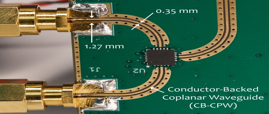
- Enhanced Grounding and Shielding: Multiple buried vias can create a dense via fence or a coaxial-like shielding structure around sensitive RF lines, effectively containing electromagnetic interference (EMI) and crosstalk.
- Facilitation of Advanced Packaging: HDI is essential for integrating embedded passive components (resistors, capacitors) and for fan-out routing from advanced semiconductor packages, keeping the entire RF front-end compact and efficient.
For RF performance, HDI is not just about making the board smaller; it’s about making it electrically superior by reducing negative effects intrinsic to larger, conventional geometries.
Key Structure and HDI Layer Configurations Used in Advanced RF Modules and Antenna Systems
The architecture of an HDI RF board is its blueprint for success. The HDI layer build-up is carefully planned to meet electrical and mechanical goals.
- Standard “1+N+1” to “Any Layer” Build-Ups: Simple HDI starts with “1+N+1” (one HDI layer on each side of a core). Advanced RF modules may use “2+N+2” or “any layer” HDI, where almost every layer can be connected with microvias, offering maximum design flexibility for complex HDI Electronics.
- Hybrid Material Stack-ups: A common configuration uses a high-performance, low-loss RF laminate (e.g., Rogers 4350B) for critical signal layers, bonded with standard FR-4 prepreg for other layers. This optimizes cost and performance.
- Buried and Blind Via Structures: Critical RF lines often reside on outer layers for best performance. Blind vias connect surface layers to adjacent inner layers without going through the entire board, preserving space and reducing stub length.
- Via-in-Pad and Filled Vias: To further miniaturize, vias are placed directly in component pads. These are plated and filled with conductive or non-conductive material, creating a flat surface for soldering and excellent thermal conduction for components like power amplifiers.
- Shielding Cavities and Antenna Structures: HDI processes can create milled cavities for shielding cans or precise, multi-layer antenna structures like patch antennas for HF RFID antenna systems, all integrated within the board itself.
This sophisticated layering is what allows a single, compact HDI RF Board to function as an entire RF subsystem.
What is HDI RF Board Price?
The HDI RF board price is not a fixed number but a variable determined by a confluence of technical factors. Understanding these helps in budgeting and design optimization.
- Board Complexity: This is the primary driver. More sequential lamination cycles, a higher count of laser-drilled microvias, and “any layer” capability increase cost significantly.
- Material Selection: High-frequency laminates (Rogers, Taconic, etc.) are far more expensive than standard FR-4. The percentage of these materials in the hybrid stack-up directly impacts the raw board cost.
- Layer Count and Size: More layers and a larger board area naturally increase material and processing time. HDI allows for smaller sizes, which can offset the cost of increased layer count.
- Specialized Processes: Costs for via-in-pad, filled vias, tight impedance control tolerances (e.g., ±5%), and advanced surface finishes (ENEPIG) add to the final price.
- Order Volume and Turnaround Time: Prototype quantities have a higher cost per unit. Production volumes bring economies of scale. Expedited fabrication also carries a premium.
As a rough guideline, expect an HDI RF board to cost 2 to 5 times more than a standard FR-4 PCB with the same dimensions and layer count, primarily due to materials and process complexity. The investment, however, is justified by the unparalleled performance and integration it enables.
Comparing HDI Electronics with Flex PCB, LED PCB, and Other Specialized Substrates for RF Applications
Choosing the right substrate is critical. Here’s how HDI Electronics compare:
- HDI RF Board vs. Flex PCB: Flex boards offer dynamic bending and space savings in assemblies. However, for core RF circuitry, standard flex materials often have higher loss tangents. HDI rigid boards provide better rigidity for component support, superior thermal management, and wider availability of ultra-low-loss laminate options. They are often used together (Rigid-Flex) where HDI areas handle the core RF processing.
- HDI RF Board vs. Standard LED PCB: A typical LED PCB prioritizes high thermal conductivity (using metal core like Aluminum) and simple circuitry to drive LEDs. An HDI RF board is focused on signal integrity at high frequencies, using different materials and complex, controlled-impedance routing. Their purposes are distinct.
- HDI RF Board vs. Standard FR-4 Multilayer: Standard multilayer boards lack the fine features and low-loss materials. They are unsuitable for high-frequency performance but are cost-effective for digital and low-frequency analog sections. HDI RF is the specialized choice for the RF front-end.
- HDI RF Board vs. Pure Ceramic Substrate (e.g., Alumina, LTCC): Ceramic offers excellent thermal performance and very fine features but at a very high cost and limited size. HDI RF on organic laminates provides a better balance of performance, size, design flexibility, and cost for most RF applications below the millimeter-wave extreme.
In essence, for the heart of a high-frequency system—where signal integrity, miniaturization, and integration are non-negotiable—the Premium HDI RF Board is the unmatched solution.
How HF RFID Antenna, RFI Board, and RDI Board Designs Benefit from HDI Technology?
These specialized applications gain distinct advantages:
- HF RFID Antenna: It is short for High Frequency Radio Frequency Identification Antenna. HF RFID antenna coils often require precise, multi-turn patterns. HDI technology allows these coils to be fabricated with extreme accuracy as embedded planar structures within the board layers, improving reliability and enabling integration with the control chip in a single, slim package.
Application: Operating at the 13.56 MHz HF band, these HDI-enabled antenna inlays or modules are critical for contactless payment systems (e.g., credit cards, mobile wallets), secure access control badges, library item tracking, and high-security document authentication. - RFI (Radio Frequency Interference) Board: Boards designed to mitigate RFI need excellent shielding. HDI allows for the easy creation of dense ground via fences and shielded cavities between noisy and sensitive sections directly within the board structure, providing superior isolation compared to external shields.
Application: Crucial for applications across a wide frequency spectrum, these boards are used in sensitive medical imaging equipment (MRI), high-density telecom infrastructure, aerospace avionics, and advanced test & measurement instruments to prevent signal degradation and ensure regulatory EMI/EMC compliance. - RDI (Research, Development, and Innovation) Boards: Prototype and RDI board projects for cutting-edge technology benefit immensely from HDI’s flexibility. It allows researchers to pack sensors, RF components, and digital processors into a small form factor for proof-of-concept devices, accelerating innovation cycles.
Application: : Used in prototyping next-generation IoT devices, millimeter-wave (mmWave) communication systems (e.g., 5G/6G fronthaul), phased array radar elements, and quantum computing interfaces, where form factor, signal integrity, and rapid design iteration are paramount.
In all cases, HDI provides the design freedom and performance consistency needed to turn advanced concepts into reliable, manufacturable products.
How to Select Reliable HDI RF Board Manufacturers?
Choosing the right partner is as important as the design itself. Look for these traits in HDI RF board manufacturers:
- Proven Technical Expertise: They must demonstrate a deep understanding of both HDI processes and RF principles (impedance, loss, materials).
- Advanced Manufacturing Capability: Verify they have laser drilling, precision lamination, and electrical testing equipment (like network analyzers) specifically for RF parameters.
- Material Partnerships: Access to a wide range of certified high-frequency laminates from leading suppliers is essential.
- Design Support Services: The best manufacturers offer upfront engineering support, including stack-up design, simulation assistance, and thorough DFM analysis.
- Quality and Certifications: Look for relevant industry certifications (ISO, IATF 16949, AS9100 for aerospace) and a robust quality management system.
Why Choose BEST Technology as One of Your Best HDI PCB Manufacturers for RF and Microwave Circuit Boards?
BEST Technology stands out by fulfilling all the above criteria and more. We specialize in the niche intersection of HDI and high-frequency, offering:
- Dual Expertise: Our engineers are fluent in the language of both advanced fabrication and RF design.
- State-of-the-Art Facility: Equipped with specialized lines for handling low-loss materials and achieving tight tolerances.
- End-to-End Partnership: We collaborate from the early design stage through prototyping to volume production, ensuring your RF and microwave circuit boards are not only designed well but are also optimized for manufacturability and yield.
- Commitment to Reliability: Every Premium HDI RF Board we build undergoes rigorous testing to meet the stringent requirements of high-reliability applications. And our PCB and SMT factory is fully compatible with ISO 9001, ISO 13485, IATF 16949, AS9100D, UL, REACH, and RoHS.
- Short Lead Times: We operate dedicated, streamlined production lines and maintain strategic raw material partnerships. This optimized workflow, combined with our deep process expertise, allows us to offer industry-leading turnaround times for both complex prototypes and volume production, enabling you to accelerate your product development and meet critical market windows without compromising on quality.
All in all, an HDI RF Board represents the pinnacle of integration for high-frequency electronics, combining the miniaturization power of HDI with the performance demands of RF circuits. This guide has explored its HDI PCB definition, benefits, structures, costs, and ideal applications to help you leverage this advanced technology for your most demanding projects.
Success in this field requires a manufacturer that is more than a fabrication house; it requires a technical co-innovator. BEST Technology brings nearly two decades of specialized HDI RF circuit board experience, cutting-edge capabilities, and a partnership-driven approach to every HDI device project. Pls feel free to contact us for a consultation or quote via sales@bestpcbs.com
FAQs
Q: What is the difference between HDI PCB and regular PCB?
- A: The main differences are density and construction. HDI PCBs use microvias (typically <150µm), finer traces/spaces, and often sequential build-up to achieve much higher interconnection density in a smaller area compared to regular PCBs that rely on larger through-hole vias and simpler lamination.
Q: What are the benefits of HDI PCB?
- A: Key benefits include significant size and weight reduction, improved electrical performance (faster signals, less noise), enhanced reliability (fewer mechanical interconnections), and the ability to accommodate advanced, high-pin-count components like BGAs.
Q: What are the 4 tiers of HDI?
A: HDI complexity is often categorized into tiers:
- Tier 1: 1+N+1 (Microvias on one side of the core).
- Tier 2: 2+N+2 (Microvias on both sides, potentially with stacked vias).
- Tier 3: 3+N+3 (Multiple layers of stacked microvias).
- Tier 4 & Above: Also called “Any Layer” HDI, where microvias can connect any two adjacent layers throughout the board stack-up.
Q: What is the process of HDI PCB fabrication?
- A: It involves sequential lamination cycles. Key steps include: imaging and etching of fine inner layers, laser drilling of microvias, via metallization (plating), layer alignment and bonding (lamination), and repeat. This differs from standard PCB fab which often uses a single lamination of all layers followed by mechanical drilling of through-holes.
Q: What is an HDI device?
- A: In the context of PCBs, an “HDI device” typically refers to the final electronic product or module that is enabled by or built upon an HDI printed circuit board, such as a smartphone, a satellite communication module, or a medical imaging device.
Tags: Best HDI PCB Manufacturers for RF and Microwave Circuit Boards, HDI RF Board, Hdi rf board manufacturers, HDI RF Board Price, HDI RF circuit board