pcb
Home > Blog

Posts Tagged ‘Assembly Services’

Ethernet Routing PCB, Fast Prototyping, Assembly Services
Tuesday, June 24th, 2025

Ethernet routing PCB is the foundation of stable high-speed networks in modern electronics. Whether you’re building routers, industrial controllers, or advanced IoT devices, the design quality directly affects performance. In this blog, we explore the essentials of ethernet routing PCB and how Best Technology helps you overcome the typical design challenges with reliable, fast, and tailored solutions.

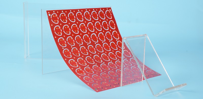
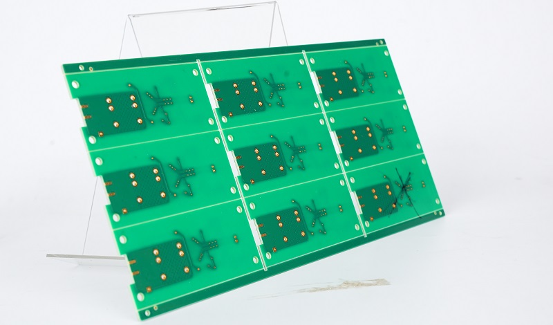
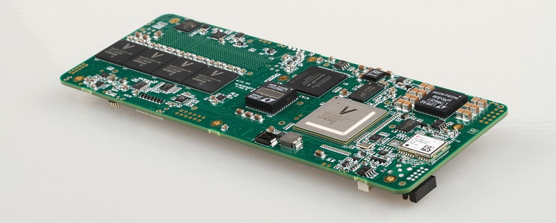
Best Technology is an ethernet routing PCB manufacturer providing high-precision ethernet routing PCB solutions with full support for up to 32-layer stack-ups. Our FR4 PCB range is varied, including single-sided PCB, multi-layer PCB, high Tg PCB, RF PCB, and so on. We are realizing that fast prototyping and one-stop assembly services are instrumental in keeping a competitive edge and winning in international markets. We appreciate the trust you gave us. Your trust is the drive for us to overcome any obstacle and provide more fast prototyping and practical solutions for your projects. Just feel free to let us know your specific ethernet routing PCB requirements via sales@bestpcbs.com.

Ethernet Routing PCB, Fast Prototyping, Assembly Services

What is Ethernet Routing PCB?

Ethernet routing PCBs are specially designed circuit boards used to manage Ethernet signal paths. These boards handle differential pair routing, impedance matching, and thermal management for high-speed data flow. They must meet tight requirements to ensure stable communication and low interference. With increasing demand for Gigabit Ethernet and 10G+ speeds, the layout needs precision from the start. Best Technology supports all design phases—from prototype to volume production—ensuring consistent quality and signal integrity.

What is Ethernet Routing PCB?

What Are the Three Types of Ethernet?

When designing an Ethernet PCB, it’s helpful to understand the core types:

  1. 10BASE-T: Basic Ethernet, up to 10 Mbps over twisted pair cable. Easy to route but outdated in many systems.
  2. 100BASE-T (Fast Ethernet): Up to 100 Mbps, still in use in some industrial and consumer systems.
  3. 1000BASE-T (Gigabit Ethernet): Up to 1 Gbps and most common today. It needs precise routing to avoid data loss.

Each type demands different impedance control, routing lengths, and connector considerations. Best Technology’s engineering team applies practical guidelines to each level, ensuring your project fits technical and budget goals.

What Is the Primary Purpose of an Ethernet Port on the Motherboard?

The Ethernet port on a motherboard serves as the physical gateway to wired networks. It connects your device to LANs or the internet, allowing stable and secure data exchange. On a PCB, the path from this port must be clean, short, and impedance-matched to maintain high-speed data transfer. We use advanced simulation tools to ensure signal fidelity, reducing EMI and enhancing long-term reliability.

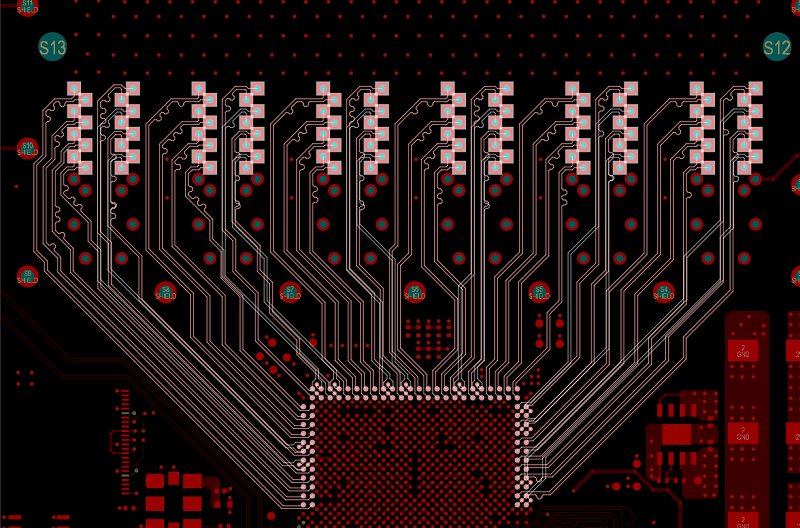
What Is the 3W Rule in PCB Routing?

The 3W rule is a layout technique to minimize crosstalk between adjacent signals. It suggests that the spacing between traces should be at least three times the width of the trace. For Ethernet, which often uses differential pairs, this rule is key to avoiding noise and maintaining clean waveforms. Our PCB layout engineers follow this rule, especially in Gigabit Ethernet sections, and combine it with proper ground shielding and return paths to improve EMC performance.

How to Properly Route an Ethernet PCB?

Proper Ethernet PCB routing means balancing signal quality, EMI reduction, thermal control, and cost. Here’s how:

  1. Impedance Matching: Use controlled impedance traces for Ethernet pairs. Keep differential pairs tightly coupled and equal in length.
  2. Minimize Crosstalk: Use the 3W rule and place pairs far enough apart. Avoid sharp bends in traces.
  3. Grounding: Keep a continuous reference ground. Prevent signal layers from crossing split planes.
  4. EMC Management: Apply filtering and shielding, especially near connectors and clocks.
  5. Thermal Management: Add thermal vias, heat sinks, or metal substrates near hot components like PHY chips.
  6. Cost Control: Optimize layer stackup and use advanced materials only where needed.

Best Technology addresses all of the above through DFM (Design for Manufacturability) checks, ensuring that your design moves to production without delays or surprises. For ethernet routing PCB solution, just feel free to give us a call at +86-755-2909-1601 or send us an e-mail at sales@bestpcbs.com.

How to Properly Route an Ethernet PCB?

How to Solve EMC Interference Issues in Ethernet PCB Layouts?

Ground plane splits and poorly shielded components often create unwanted radiation. Best Technology prevents this by maintaining a uniform ground plane, shrinking power layers, and using ferrite beads or shielding cans around sensitive areas. This helps your design pass EMC testing quickly, saving you costly redesigns and delays.

Gigabit Ethernet devices often use high-power ICs that create local heat. To deal with this, we place heat vias beneath chips, use thermal interface materials, and sometimes recommend metal-backed PCBs. These techniques ensure your board stays cool even under heavy data load. We also provide aluminum substrate options when heat becomes a critical challenge.

Why Choose Best Technology for Ethernet PCB Manufacturing?

  • Excellent Layer Count and Material Compatibility. Our production supports up to 32 layers, with high-Tg FR4 and advanced materials like Rogers 4350, Isola 370HR, and Megtron series, offering flexibility for high-speed differential pair routing and EMC shielding design.
  • Turnkey Ethernet Routing PCB Solutions. Many customers come to us after facing delays, EMC failures, or thermal issues in early prototypes. We offer the solutions they need: fast, precise, and certified. From layout optimization to advanced testing, we cover all bases. Our engineers also understand how to reduce costs without sacrificing results—making us a trusted partner across industries from telecom to automotive.
  • Rapid Prototyping Services. Our team offers fast-turn services, delivering working Ethernet routing PCBs in 5–7 days. We support quick revisions and cost-efficient builds so you can iterate and validate your product fast. That helps reduce time to market and allows real feedback from customers.
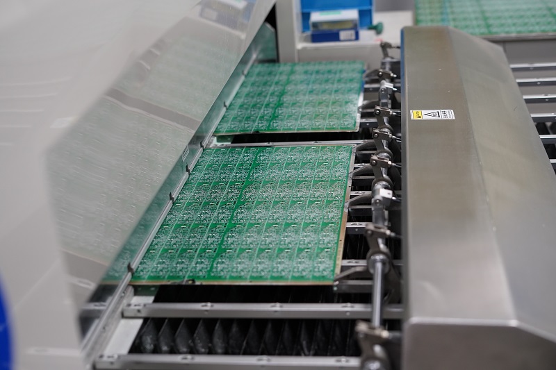
  • Professional Assembly and Testing. Best Technology uses advanced equipment for SMT and through-hole processes, ensuring that even high-density layouts meet spec. We also perform full functional and AOI testing, X-ray for BGAs, and final verification before shipment. Our services comply with ISO9001, AS9100D, and other key standards.
  • Advanced Surface Finishes for High Reliability. Options like ENIG, immersion silver, OSP, and hard gold are available, ensuring excellent surface planarity and oxidation resistance for high-speed Ethernet connector pads.
Why Choose Best Technology?

In summary, designing an Ethernet routing PCB is not just about connecting pins—it’s about performance, reliability, and speed. With Best Technology, you get a partner who understands signal integrity, EMC, thermal control, and cost balance. Our fast prototyping, flexible assembly, and strict quality control help ensure your product succeeds—from the first prototype to mass production. Please feel free to e-mail us directly at sales@bestpcbs.com for a viable solution for Ethernet routing PCB layout.

You may also like

PCB Fabrication China, Rapid Prototyping, Assembly Services
Monday, June 23rd, 2025

PCB fabrication china is more than a search term; it is the door to a huge ecosystem that blends speed, skill, and cost‑effectiveness. In this guide you will see how Chinese plants turn design ideas into reliable boards, how rapid prototypes cut weeks off a schedule, and how assembly services let you launch products sooner. You will also meet Best Technology, a factory that fixes your needs with practical solution.

Best Technology provides PCB fabrication, rapid prototyping, and assembly services in China. High-mix, low-volume, high-quality, fast prototyping, and turnkey assembly service are our core competencies. Our wide PCB range includes FR4 PCBs, ceramic PCBs, and metal core PCBs. Just feel free to contact us via sales@bestpcbs.com for effective solutions for your PCB fabrication projects.

PCB Fabrication China, Rapid Prototyping, Assembly Services

What Is the Best PCB Fabrication China Company?

Every engineer wants the “best,” yet that word means different things. Some value dense HDI layers, some need medical traceability, and others just want parts shipped fast. In China the list of factories is long, but only a few check every box. The best partner masters three areas at once: production management, technical design help, and delivery quality. Clear planning tools avoid the last‑minute schedule chaos that plagues many shops. A digital MES platform logs every panel and keeps data honest. A customer sees real‑time status and can adjust volumes without fear of hidden delays. That is how Best Technology has built trust. Its engineers run early DFM reviews, spot Mark point gaps, and resize tiny test pads that slow AOI. When boards ship, each has a QR code that links to full trace records. The “best” is not just clean copper; it is also calm communication, stable lead times, and data you can show your own clients.

PCB Fabrication China

PCB Fabrication Manufacturer in China

China hosts thousands of board shops, yet the market sorts itself into clear tiers:

Tier‑1 Integrated Groups. These giants run multiple plants, own laminate lines, and serve telecom or server farms. They tackle high‑layer counts but may give prototypes low priority.

Tier‑2 Specialist Plants. Focus areas include RF, ceramic, or flex. They invest in niche gear and skilled staff. Best Technology sits here, pairing fine‑line know‑how with agile service.

Tier‑3 Mass Producers. They chase large consumer orders. Prices are sharp, yet service is thin and design feedback minimal.

When you need both speed and precision, the specialist tier wins. Best Technology uses small‑batch parallel lines, so one day it runs a six‑piece RF sample, the next day a thousand power boards. The team holds ISO 9001, ISO 13485, IATF 16949, and AS9100D certificates. These cover medical, automotive, and aerospace fields, letting customers merge different projects under one roof rather than juggle several vendors.

Who Is the Largest PCB Fabrication China Supplier?

Measured by revenue, the crown often shifts between names such as Wus, Shennan, and DSBJ, each topping billions of dollars in sales. Their size brings depth of process but also layers of approval that can slow tweaks. For small to mid runs you may wait in a queue behind telecom giants. That gap is where agile factories thrive. Best Technology may not be the biggest by floor space, yet its smart line layout and lean cells give response speed that giants cannot match. A focused scope means a project manager can tweak a drill file this morning and still plate copper tonight. Growth is steady but controlled, so each client keeps a direct contact, not a ticket number in a help desk.

Is Best Technology in China?

Yes. Best Technology is head‑quartered in Shenzhen. The site sits close to laminate suppliers like Shengyi, logistics hubs in Shenzhen, and the port of Hong Kong. That location drops transit time and lets engineers visit raw material plants the same day an issue appears. For customers abroad this means shorter DHL routes and consistent freight rates. Local teams speak fluent English, which clears cultural hurdles and streamlines calls.

How Much Does PCB Fabrication China Cost?

Cost moves with layer count, copper weight, surface finish, and above all, order volume. A two‑layer FR‑4 sample under 100 mm² may cost under USD 30 shipped air. Move to eight layers, blind vias, ENIG finish, and that price rises toward USD 150 for the same outline. Volume orders drive price per piece down fast once panels fill the full 18 × 24 inch sheet. Best Technology gives sliding scales on each quote, so design teams see break‑even points between prototype and pilot runs. The quote also lists lead time options if you need: standard and express. Express lifts cost a little but the urgent boards can be finished within 24 hours. All fees appear in one sheet—fabrication, parts, SMT set‑up—so buyers avoid hidden extras later.

What Is the Most Commonly Used PCB Material in PCB Fabrication China?

Standard FR‑4 remains the workhorse due to balanced strength, thermal limits, and price. For flex layers, PI (polyimide) is top. High‑frequency lines move toward low‑loss Rogers 4350B or Shengyi S1000-2. Ceramic boards use alumina or aluminum nitride for LED cooling. Best Technology stocks key grades from local and global brands. A buffer stock policy keeps two weeks of common cores and coppers on hand, which shields your schedule from sudden laminate shortages.

What Is the Most Commonly Used PCB Material in PCB Fabrication China?

Why Should You Choose Best Technology as Your PCB Fabrication China Partner?

1. It clears design snags fast. Mark points off the grid? V‑score too deep? In‑house CAM engineers spot the glitch, send a marked Gerber back within two hours, and jump to drill only after you approve.

2. It tracks every board. A laser QR at final AOI links drill bits, plating bath ID, and solder mask batch. If a field failure occurs, you view root data at once. That cuts RMA cycles and builds end‑customer trust.

3. It levels up assembly. Fabrication and SMT share one floor, so panels stay indoors. Parts pass X‑ray, then SPI, then reflow in a nitrogen oven. Mixed‑tech builds place BGA on side A, then through‑hole on side B, soldered by selective wave. A final functional jig runs power‑up and boundary scan.

4. It guards quality. Certifications cover ISO 9001, ISO 13485, IATF 16949, and AS9100D. Audits by medical and aerospace clients verify processes each year.

Why Should You Choose Best Technology as Your PCB Fabrication China Partner?

In summary, choosing a PCB fabrication china partner is no longer a game of rock‑bottom price. True value lies in smart planning, reliable quality, and rapid prototyping that keep your design moving. Best Technology answers each of your demands—plan shifts, design hurdles, and traceability—through an MES backbone, on‑site assembly, and a culture of open talks. Offering high-quality PCBs is the prerequisite for us to gain the trust of both potential clients and regular customers. And good and prompt service is our soft skill. Reach out to us and share your Gerbers with us at sales@bestpcbs.com, and feel the difference on your very next project.

You may also like