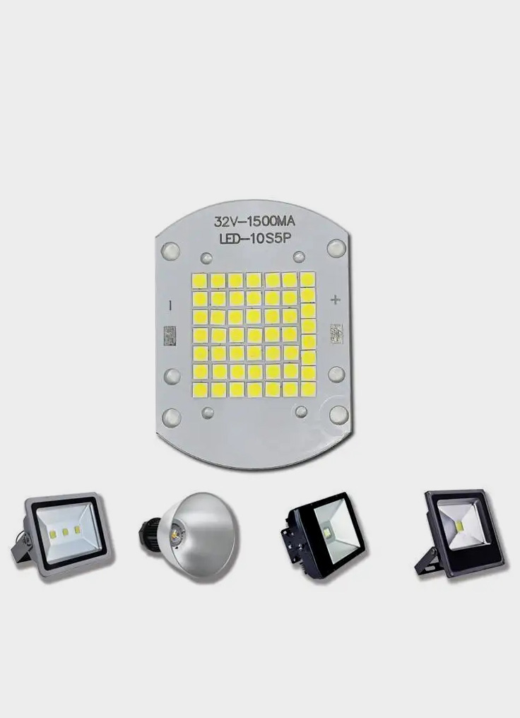
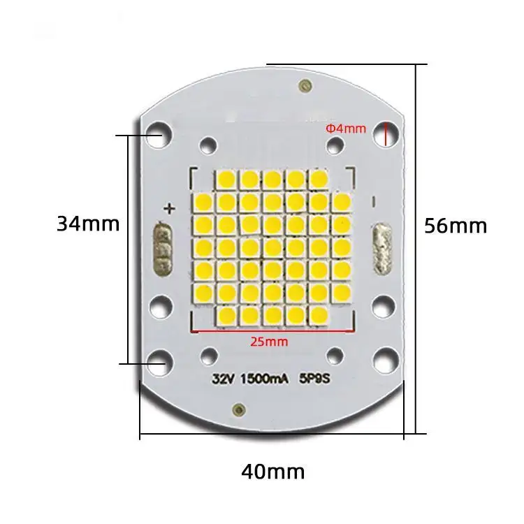
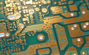
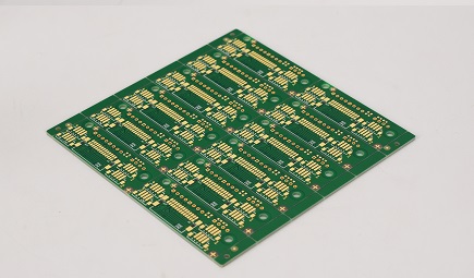
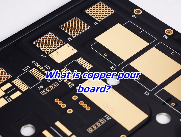
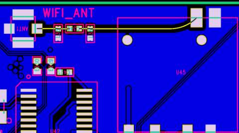
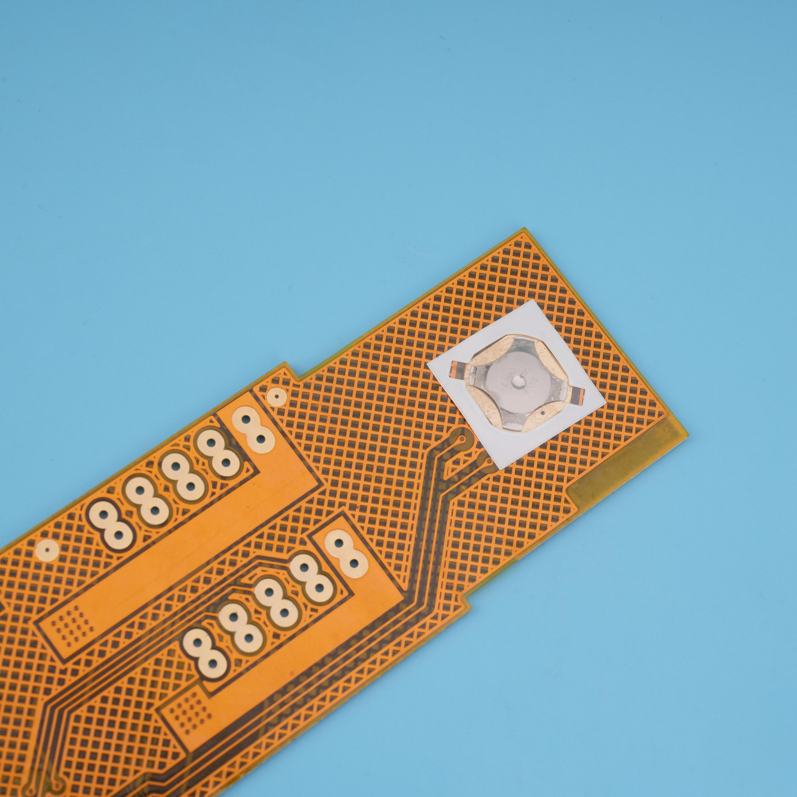
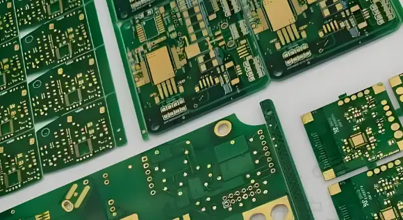
What is a single-sided PCB circuit board
Single-sided PCB circuit board is a type of printed circuit board. Only one side of the PCB board has circuits (it can have holes or not), and the other side is a substrate or directly covered with insulating ink. There is no circuit and the whole board is transparent under strong light (except for individual boards and special process requirements). The cross section only contains copper foil on the side with circuits.
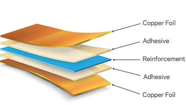
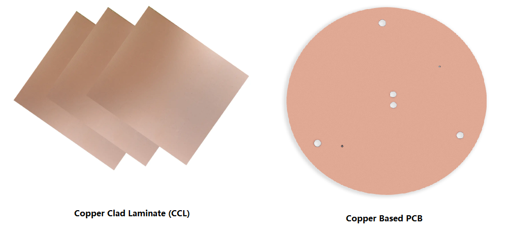
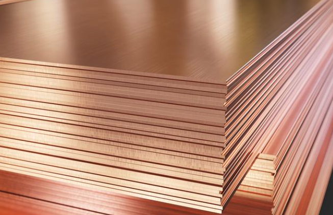
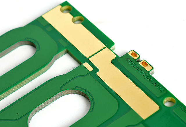
Single-sided PCB circuit board is obtained by etching copper-clad board. Copper-clad board consists of board base and copper foil. The board base is usually made of insulating materials such as glass fiber, and is covered with a layer of copper foil (usually oxygen-free copper).


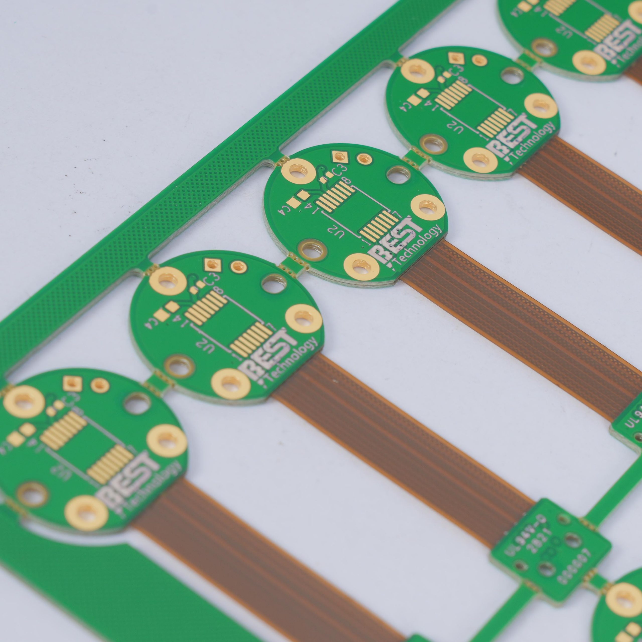
Single layer PCB manufacturer
Single layer PCB manufacturer Best Technology has offered high-quality PCBs and the best PCB assembly & box building service all over the world since 2006. We are professional fabricator on PCB prototype, IPC Class III standard are available. You can get high-quality PCB board and PCBA at a very reasonable price.
Single layer PCB design
Best Technology excels in PCB design, perform PI analysis, SI analysis, EMC test and DFM tests to ensure one-time successed PCB design. Over 20 professional engineers, all of them has more than 15+ years experience in PCB, we make sure every design is optimized for performance and manufacturability.
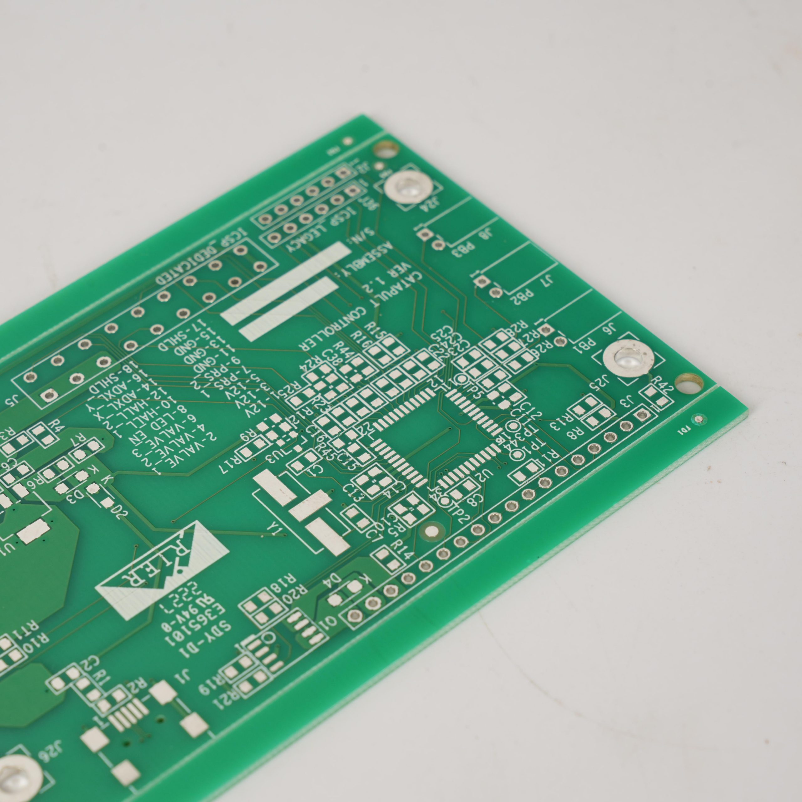
Single layer PCB prototype
As an industry-leading PCB prototype manufacturer, Best Technology offers 24 hours quick turn PCB prototype, PCB assembly and reliable small-batch PCB production. Free technical support and VIP one-to-one service.
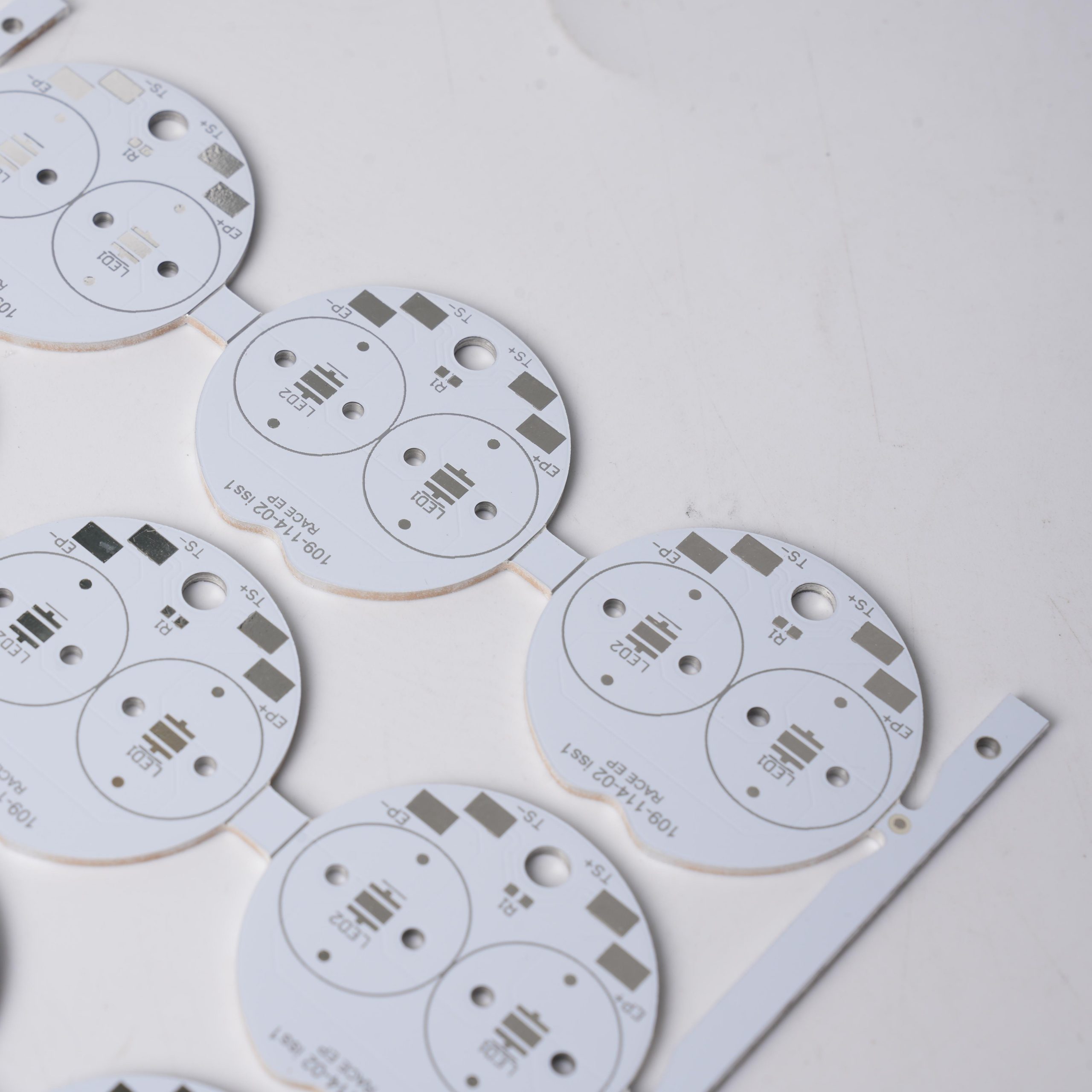
Single layer PCB production
With over 18 years PCB manufacture experience, we dedicated to provide highest quality PCB for customers. We offer turnkey service from PCB design, PCB layout, PCB prototype, mass production and PCB assembly. Contact us to get an instant quote.
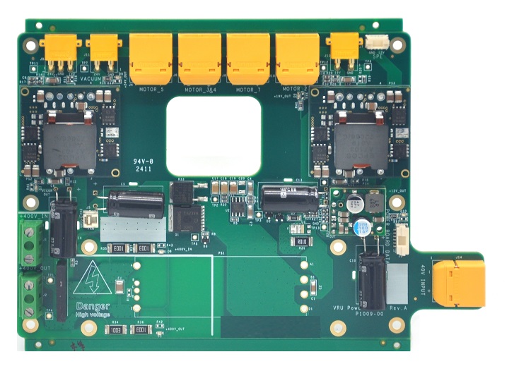
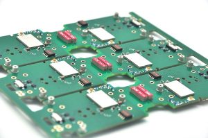
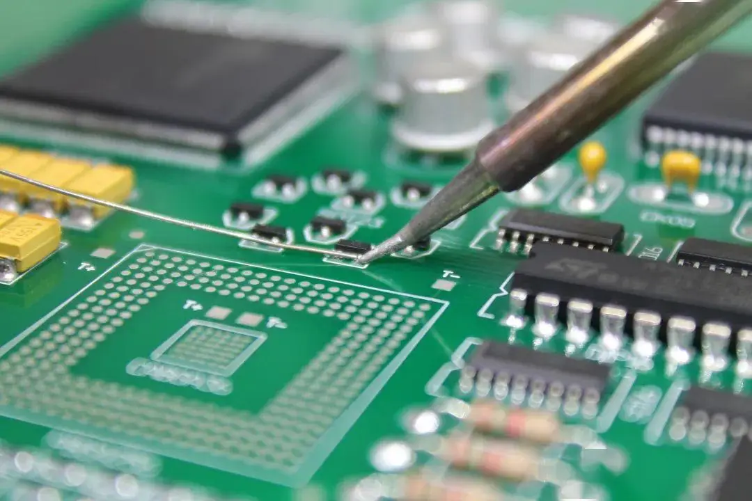
Single layer PCB assembly
Professional PCB assembly service, includes DFM/DFA checks, function/ICT testing, X-RAY, Online dual AOI, nitrogen reflow oven. 10+ SMT lines, free passive parts and Thorough Inspections! SMT, Thru-hole, BGA, QFN Assembly at Low Prices! No MOQ, complex and difficulty designs welcome!
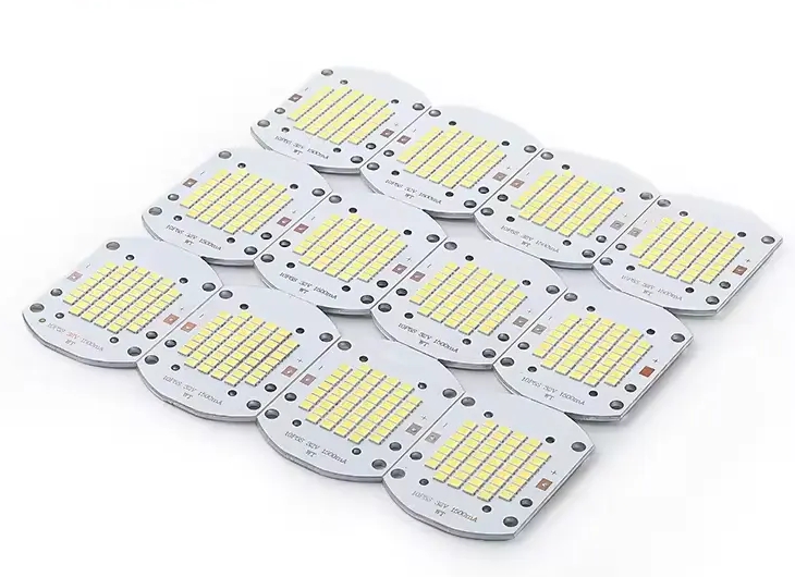
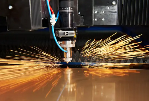
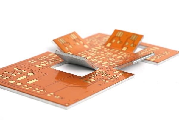
Single-sided PCB production process
- Cutting
- Drilling or punching
- Screen printing circuit anti-etching pattern or using dry film
- Curing inspection and board repair
- Screen printing solder mask pattern (commonly used green oil)
- Screen printing character mark pattern, UV curing
- Preheating, punching and appearance
- Electrical open and short circuit test
- Pre-coating flux anti-oxidant (drying) or tin spraying hot air leveling
- Packaging and delivery
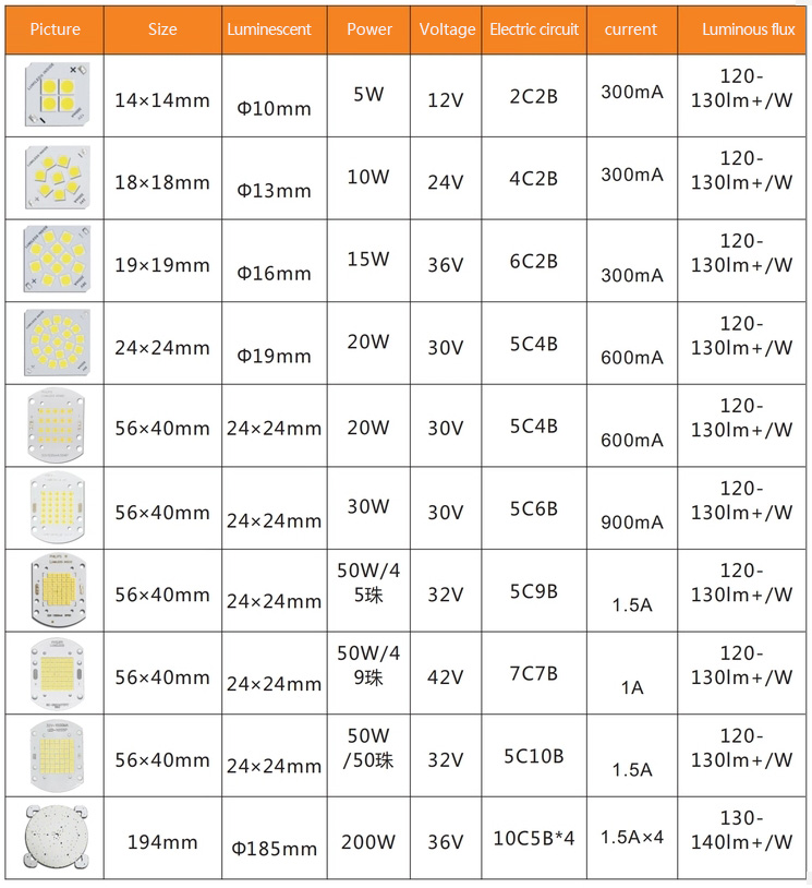
Single-sided PCB production capacity
| Item | Content |
| Material type : | XPC FR-1 FR-4 CEM-1 |
| Surface finish : | ENIG gold, HASL Immersion Tin, Chemical Silver OSP |
| Layer No : | Single side, Multilayer PCB |
| Max PCB size: | 1500mm*600mm |
| Min PCB size: | 5mm*5mm |
| Min space/width: | 0.1mm |
| Warp and Twist: | ≤0.5%(board thickness:1.6mm,PCB size : 300mm*300mm) |
| Board thickness: | 0.3-5.0mm |
| Copper thickness: | 35um-240um |
| Outline Tolerance: | ±0.15mm |
| V-CUT Precision: | ±0.1mm |
| Capacity: | 80000㎡/Month |
| PTH Dia tolerance: | ±0.076mm |
| Outline tolerance: | CNC :±0.1mm punch:±0.15mm |
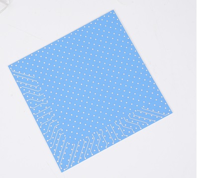
What are the single-sided PCB materials?
What are the single-sided PCB materials
Phenolic paper substrate
Phenolic paper substrate (commonly known as cardboard, plastic board, V0 board, flame retardant board, red-letter copper clad board, 94V0). The most commonly used product models of phenolic paper-based copper clad boards are FR-1 (flame retardant) and XPC (non-flame retardant). Single-sided copper clad boards can be easily judged from the color of the characters on the back of the board. Generally, red characters are FR-1 (flame retardant) and blue characters are XPC (non-flame retardant). This type of board is the cheapest compared to other types of boards.
Epoxy fiberglass cloth substrate
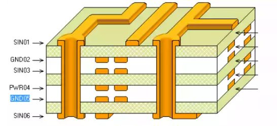
Epoxy fiberglass cloth substrate (commonly known as: epoxy board, fiberglass board, fiberboard, FR4), epoxy fiberglass cloth substrate is a type of substrate with epoxy resin as adhesive and electronic grade glass fiber cloth as reinforcing material. Its bonding sheet and inner core thin copper clad board are important substrates for making multi-layer printed circuit boards. The working temperature is high and its own performance is less affected by the environment. In terms of processing technology, it has great advantages over other resin fiberglass cloth substrates. This type of product is mainly used for double-sided PCBs. It is also about twice as expensive as phenolic paper substrates, and the commonly used thickness is 1.5MM.
Composite substrates
Composite substrates (commonly known as powder boards, etc., cem-1 boards are also called 22F in some places in China) mainly refer to CEM-1 and CEM-3 composite-based copper-clad boards. Copper-clad boards made of wood pulp fiber paper or cotton pulp fiber paper as core reinforcement materials and glass fiber cloth as surface reinforcement materials, both of which are impregnated with flame-retardant epoxy resin, are called CEM-1. Copper-clad boards made of glass fiber paper as core reinforcement materials and glass fiber cloth as surface reinforcement materials, both of which are impregnated with flame-retardant epoxy resin, are called CEM-3. These two types of copper-clad boards are the most common composite-based copper-clad boards. This type of board is cheaper than FR4 type boards.
Single-sided PCB circuit board price
Since the cost of single-sided PCB circuit boards is affected by many factors, including the cost of raw materials, production cost, production process, special requirements, etc., its exact pricing needs to be negotiated with its single-sided PCB circuit board supplier. The general unit price calculation formula is: (length MM) × (width MM) × 0.01 × unit price (yuan/square meter) ÷ 10000 (rounded to 3 decimal places)
For specific single-sided PCB quotes, please consult bestpcbs.
Single-sided PCB circuit board price
Single-sided PCB applications and features
Single-sided PCBs are increasingly widely used due to their many unique advantages;
High density: For decades, high-density printed boards have developed with the improvement of integrated circuit integration and the advancement of installation technology.
High reliability: Through a series of inspections, tests and aging tests, PCBs can work reliably for a long time (usually 20 years).
Designability: According to the requirements of various performances (electrical, physical, chemical, mechanical, etc.) of single-sided boards, printed boards can be designed in a short time and efficiently through design standardization.
Manufacturability: Through modern production management, standardization, scale (quantification), automation, etc. can be achieved to ensure the consistency of product quality.
Testability: Complete test methods, standards and various test equipment and instruments have been established to detect and evaluate the qualification and service life of a single PCB.
Assembly: Circuit boards facilitate standardized assembly of various components to achieve automated, large-scale mass production. At the same time, circuit boards and various component assemblies can be assembled into larger components and systems, and even complete machines.
Maintainability: Circuit boards and various component parts are manufactured with standardized designs and scales. If a system fails, components can be replaced quickly and conveniently. The system can recover quickly due to this flexibility. More examples include system miniaturization, lightweight, high-speed signal transmission, etc.
FAQ About single sided pcb
FAQ About single sided pcb
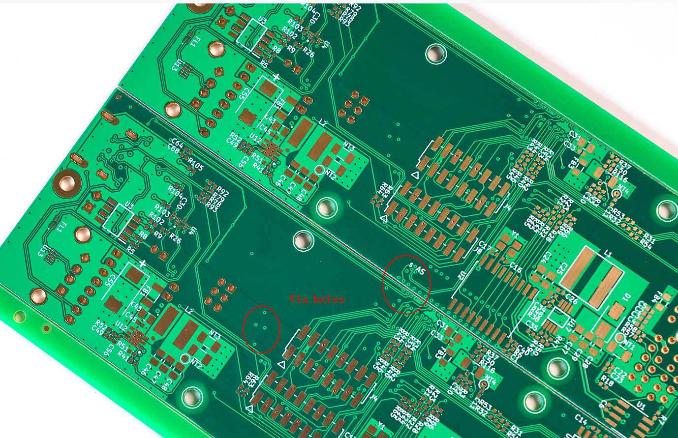
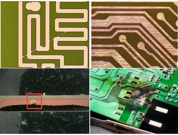
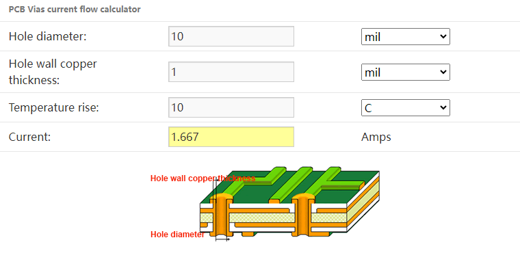
Q: When laying out the board, if the lines are dense, there may be more vias, which will of course affect the electrical performance of the board. How can I improve the electrical performance of the board?
A: For low-frequency signals, vias are not a big deal, but for high-frequency signals, try to reduce vias. If there are many lines, you can consider multi-layer boards;
Q: Is it better to add more decoupling capacitors on the board?
A: Decoupling capacitors need to be added with appropriate values at appropriate locations. For example, add them to the power supply port of your analog device, and use different capacitance values to filter out stray signals of different frequencies;
Q: What are the standards for a good board?
A: Reasonable layout, sufficient power redundancy of power lines, high-frequency impedance, and simple low-frequency routing.
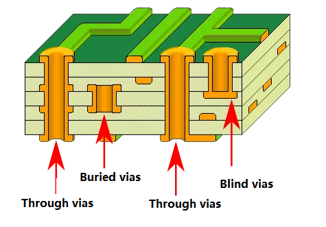
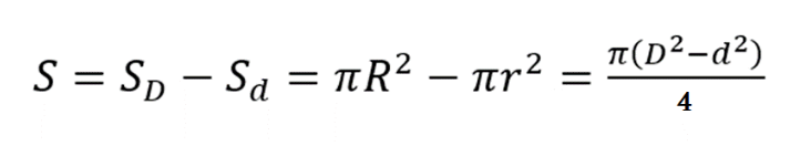
Q: How much difference do through holes and blind holes have on signals? What are the application principles?
A: Using blind or buried holes is an effective way to increase the density of multi-layer boards, reduce the number of layers and board size, and greatly reduce the number of plated through holes. But in comparison, through holes are easy to implement in terms of process and have lower costs, so through holes are generally used in designs.
Q: What kind of layout can achieve the best heat dissipation effect?
A: There are three main sources of heat in PCB: (1) heat generated by electronic components; (2) heat generated by the PCB itself; (3) heat transmitted from other parts. Among these three heat sources, the heat generated by components is the largest and is the main heat source, followed by the heat generated by the PCB board. The heat transmitted from the outside depends on the overall thermal design of the system and is not considered for the time being. The purpose of thermal design is to take appropriate measures and methods to reduce the temperature of components and PCB boards so that the system can work normally at a suitable temperature. This is mainly achieved by reducing heat generation and accelerating heat dissipation.
Q: Can you explain the proportional relationship between the line width and the size of the matching via?
A: This is a good question. It is difficult to say that there is a simple proportional relationship because the two simulations are different. One is surface transmission and the other is ring transmission. You can find a via impedance calculation software on the Internet, and then keep the impedance of the via consistent with the impedance of the transmission line.
Q: In an ordinary PCB circuit board with an MCU control, but without high current and high-speed signal requirements, is it better to lay a layer of ground wire around the outermost edge of the PCB to wrap the entire circuit board?
A: Generally speaking, just lay a complete ground.
Q: How to deal with the avoidance of vias during the wiring process of high-speed PCB, what good suggestions are there?
A: For high-speed PCB, it is best to make fewer vias and solve the need to increase vias by adding signal layers.
Q: How to select the thickness of the power trace in PCB board design? Are there any rules?
A: You can refer to: 0.15×line width (mm)=A, and copper thickness also needs to be considered.
Q: When digital circuits and analog circuits are on the same multi-layer board, should analog ground and digital ground be arranged on different layers?
A: This is not necessary, but analog circuits and digital circuits should be placed separately.
Q: How many vias are generally suitable for digital signal transmission? (Signals below 120Mhz)
A: It is best not to exceed two vias.