Archive for December, 2022

How to choose surface finish on Printed Circuit Board?

Saturday, December 17th, 2022

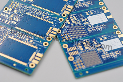
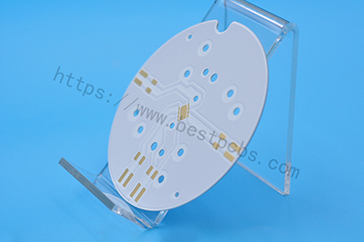
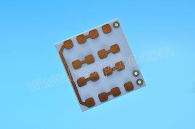
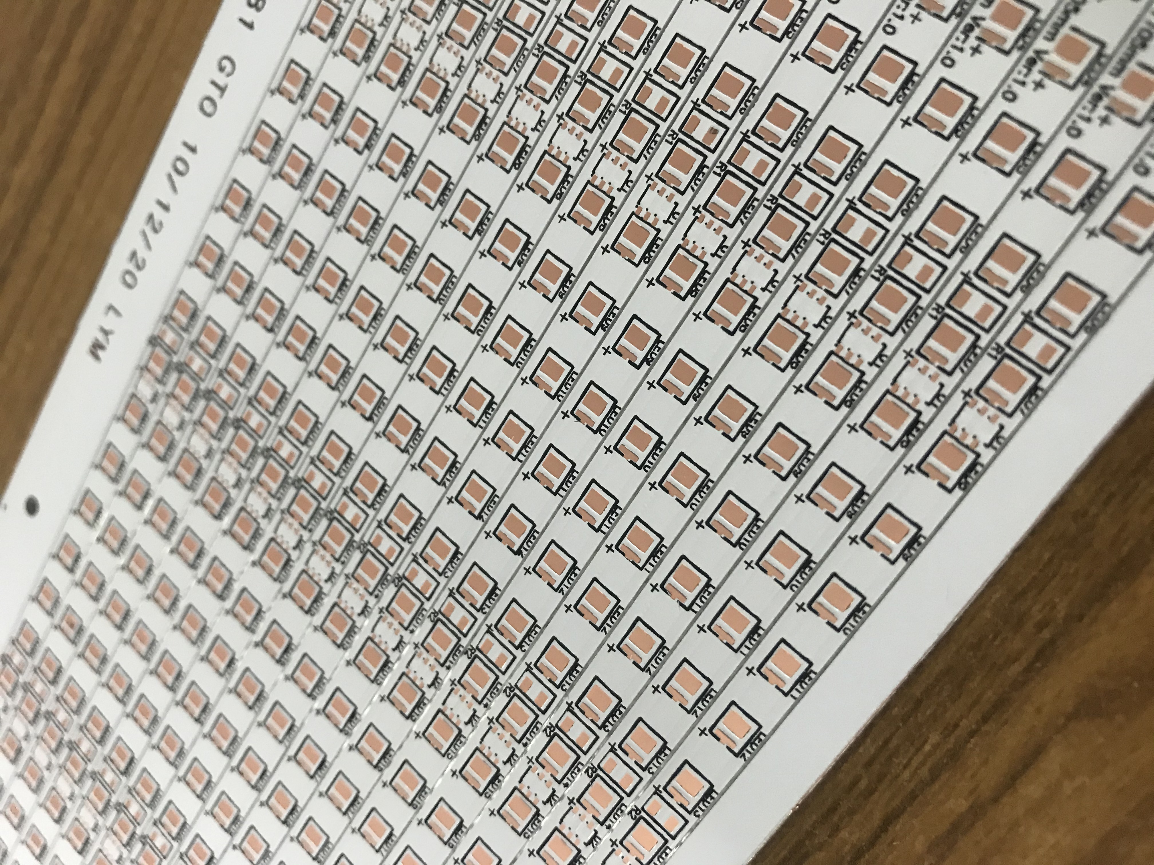
When finish the PCB design, we should choose a suitable surface finish to protect traces from corrosion. Nowadays, the most popular surface treatments for PCB manufacturer to use are HASL/LF HASL, OSP and ENIG.

Different surface treatment has its unique functionality and the cost also is different. This article we will show you the pros and cons of the three surface finishing which use while the PCB manufacturing process.

HASL Surface Finish

HASL (Hot Air Solder Level) can be known as tin-lead HASL and lead-free HASL, it was the mainstream surface treatment technology in the 1980s, but with the increased of “small and high density” demands in PCB, there are less and less circuit boards use the HASL technology because it will cause the defective products due to the solder point are easy to leave on the board surface during SMT process. In view of this situation, some PCB board manufacturers or designers prefer use OSP or immersion gold to ensure the good quality products as well as smooth production process.

  • Tin-lead HASL

Advantages:

1) Economical and widely available.

2) Excellent solderability.

3)Better mechanical strength & lustrousness than lead-free HSAL.

Disadvantages: it is harmful to environment and violates RoHS compliance.

  • Lead-free HASL

Advantages: low cost, good solder performance and environmental.

Disadvantages: mechanical strength & lustrousness are not good than lead HASL.

In additional, due to the poor surface flatness of HASL circuit boards, neither leaded nor lead-free HASL is not suitable for soldering fine-pitch components or plated through-holes, because it will cause the short circuits and poor welding during the assembly process.

(LF_HASL)

OSP

OSP (Organic Solderability Preservatives) also named as pre flux, the working principle is to generate a layer of organic film chemically on the copper surface to protect the surface from oxidation or vulcanization in the room environment. Meanwhile, OSP also can increase the oxidation resistance, heat shock resistance and moisture resistance of a PCB. 

OSP is equivalent to an anti-oxidation treatment, the protective thin film can be easily removed by the flux quickly under the high soldering temperature, then it makes the exposed copper surface immediately combined with the molten solder in a very short time to become a solid solder spot.

At present, the usage of OSP surface finishing process has increased significantly because it is appropriated for both low and high-end products. If your application has no surface connection functional requirements or storage life limitations, the OSP process is the most desirable surface treatment process.

(OSP_surface_treatment)

Advantage:

1)With all the advantages of bare copper soldering, expired (more than 3 months) boards can also be resurfaced, but one time is better.

2)Good for fine-pitch, BGA and smaller components.

3)Low cost and easy to rework.

4)Simple process and easy to ensure quality.

Disadvantage:

1)OSP is easily affected by acid and humidity, so must be packed with vacuum.

2)Need to do surface treatment again if storage time more than 3 months.

3)It should be used within 24 hours after unpacking.

4)OSP is an insulating layer, so the test point must be printed with solder paste to remove the original OSP layer for electrical testing.

ENIG

ENIG (Electroless Nickel/Immersion Gold) is one of a chemical nickel gold deposition method, the working principle is to generate a layer of coating by chemical REDOX reaction to get a thicker gold layer. Currently, ENIG is mainly used in the surface of the circuit board with connection functional requirements and long storage life.

Advantage:

1)Can be stored long time as well as no oxidation.

2)Good flatness surface and suitable for small solder point components.

3)Good solderability.

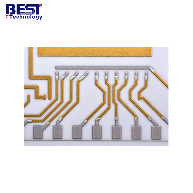
4)Can be used as the base material for COB wire bonding.

Disadvantage:

1)High cost than other two surface treatments.

2)Easy to exist black-pad issue during production process.

(ENIG)

As we can know from above information, each PCB surface treatment has its own merit and demerit, you can choose the one according to the effect you want to reach, as well as your cost. 

If you don’t know which is best for you, you can send inquiry to us, our professional engineering team and PCB sales will choose the suitable one for you. Welcome to contact us if you have any other questions.

You may also like

How To Make PCB Silkscreen on Automatic Silkscreen Printer

Thursday, December 8th, 2022

If you’ve ever learned a printed circuit board, you may see some silkscreen legends printed on the PCB. Silkscreen legend plays an important role in PCB production process.  Therefore, the quality of silkscreen also is significant.

(Silkscreen)

Last time we share some acknowledges about silkscreen guideline, today we will introduce how to make PCB silkscreen on the Automatic Silkscreen Printer step by step for you.

Manufacturing processes of printing silkscreen

  • Screen fix

Step 1, we need to fix the screen on the base or workbench with a fixture, and leave 3-5mm distance away from the positioning plate when put the screen.

  • Align and position

Step 2, we need to place the circuit board on the positioning plate with right-angle positioning method or stud registration method (generally use 2 positioning pieces), make it fixed and aligned, then put down the stencil frame and adjust the positioning button, so that the PCB outline is roughly overlapping with screen. Next step, perform initial align boards according to the positioning holes or outline line, then gradually adjust to the optimal position based on pads.

  • Silkscreen ink selection and fine-tune

Step 3, we need to select the silkscreen ink according to the customer requirements, put down the screen frame and poured ink into the screen frame, and then select the length of the appropriate scraper for trial printing sample, and fine-tune the positioning until accurate. 

  • Trial printing

Step 4, we will need to do trial printing the prototypes with transparent character alignment film and check to see if there is a legend deviation, if no, then we can proceed with mass production, but if not, then the positioning should be fine-tuned again, rip off the defective film and affixed with the new one then printing again, repeat trail until qualified.

(Trail_printing_inspection)
  • Screen printing (manually)

Step 5, let’s place the circuit board (which have finished surface treatment process) on a fixed position, put down the screen frame, and then hold the scraper with both hands, at an Angle of 50°- 60 ° with even force on the scraping screen surface from front to back or from back to front. The printing material is subjected to the pressure of the scraper through the printing mesh hole and printed on the circuit board. After the scraper passes through, the screen recovers by its own tension. After the scraper is finished, the screen frame is lifted, and the sealing screen printing material is scraped back.

  • Screen printing (auto printer)

Step 6, the Angle of the scraper is an external “eight” font, usually between 20-30 degrees, you can choose the printing times according to the actual needs.

(Auto_printing)

In the past, most of the factories make the screen printing manually, it is time consuming and limited to relatively short lengths of 60 yards. So, in our manufacturing line, we have imported the automatic flat-bed screen printing.

Automatic_Silkscreen_Printer

Here I would like to share some features of the PCB silkscreen printer with you:

Features of Auto-Printer

  • High speed: the automatic screen printer has its own unique frequency conversion speed regulation device, the printing speed can be adjusted from 20 to 70 times per minute auto screen printing machine.
  • Cost-effective: the auto printer has its own electronic counter, which can automatically shut down according to the pre-designed total number, saving a lot of manpower and ink material.
  • Good quality: the automatic screen printer is very accurate in point and color, because it is equipped with a multi-color printing electric eye device, which can improve the quality of printing.
  • Good adhesive: the adhesion of the screen machine is very good, and the ink layer is relatively thick, so the text legend is not easy to fade.
  • Multi-aspect: the fully automatic screen printer can not only be used alone, but also can be connected to a UV dryer, or a slitting machine, a reminder, and other auxiliary machines.

With the help of Automatic silkscreen printer, we are able to provide “faster” and more “efficient” service to our customers, warmly welcome to contact us, we are ONLINE always!

You may also like

Why Printed Circuit Boards are Important for Electronics?

Wednesday, December 7th, 2022

Printed Circuit Boards are the core of the electronics devices, and they exist in everywhere and be everything from your electronic equipment such as mobile phone, computers, so what are they? Let’s explore the secrets together and know why they become more common as technology advances.

What are Printed Circuit Boards?

A printed circuit board also known as PCB for short, is an electronic board for connecting metal circuits by mounting different electronic components in a device and have it do its functions.

PCB is made of fiberglass and laminate materials or a composite epoxy with conductive, it can be made to varies shapes and sizes depends on what applications it will be used for—some have many holes on it while some only have several pads or traces.

In most of devices, we can see there are many components or wires mounted or connected on the surface of PCB, which comes into two different pathways –surface mount and through-hole. Surface mount is a technology that can be abbreviated as SMT, it is a famous technical that mount electronic components (typically SMDs) attached on top of a pad by melted solder paste. Through-hole generally refers to components that have wires through the plated-through-holes that drilled into the circuit board. Both ways are commonly use, but currently with the fast development of the technology advance, surface mount is more popular than through-hole as it is more convenient for production.

What the Functions of Printed Circuit Boards?

The main functions of a PCB is to connect different components and achieve a communication between components and devices, that can be used for everywhere you can think of – Computer, phones, televisions, tablets, cameras, projectors, and so on….

For a simple example, a phone has a PCB that can connect screen, the buttons, cameras, and the circuits on the both sides. Without this board, those components wouldn’t be able to transmit signals and talk to each other and the phone would cease to function.

In addition, electronic equipment using printed board enable to avoid the error of manual wiring, and can realize the automatic insertion or installation of electronic components, automatic soldering, automatic detection by communicate with each other, to ensure the quality of electronic products, improve labor productivity, protect components from damaged, reduce costs, and easy to maintenance.

The advantages of Printed Circuit Boards

PCB performs a number of advantages in electronic industries, a most significant feature is they make products be smaller and more portable as its density circuits and components communication. The density circuits on PCB allows it take up much space for components so you can get a smaller product.

  • High density

Over the past decades, the high density of printed boards has been developed with the improvement of integrated circuits and the advancement of installation technology.

  • High reliability

Through a series of checks, tests and aging tests, the PCB can be guaranteed to work reliably for a long time (generally 20 years).

  • Designability

For various performance (electrical, physical, chemical, mechanical, etc.) requirements, can PCB be achieved to such requirements in short time and high efficiency according to design standard rules.

  • Maintainability

By means of standard PCB design rules, once the program or device failure, users fix the devices quickly.

  • Cooling abilities

Overheating is one of the biggest reasons of electronics failure, so by keeping them cool with a PCB, you can increase the lifetime of your product.

Types of Printed Circuit Boards

Best Technology provides different kinds of PCBs and PCBAs for our customers, for a quickly reviewing, we listing as below:

  • Rigid Printed Circuit Board (FR4-PCB)
  • Flex Printed Circuit Board (FPCB)
  • Rigid-Flex PCB
  • Metal Core Printed Circuit Board (MCPCB)
  • Ceramic Board
  • SinkPAD Board
  • Other special PCB such as heavy copper PCB, HDI PCB, RF PCB, and so forth
  • PCB assembly

In a word, with the development of electronics, it’s necessary to have a functional part like the PCB that can keep up with the demand. Next step, contact us if you have PCB demands.

You may also like

Differences Between Solder Mask and Solder Paste in PCB

Wednesday, December 7th, 2022

When it comes to solder mask and solder paste, there are some engineers confused about their functionalities and even most of laymen thought they are the same, this is not hypothetical, it is real that happened to me. So today let’s explain differences between Solder Mask and Solder Paste for you.

Part 1: What is Solder Mask?

If you had ever seen a printed circuit board, you may see there is a layer of green ink cover on the PCB surface while some orange-yellow areas didn’t cover by ink. In PCB industry, the green ink we called Solder Mask, or abbreviated as S/M, and exposed area is copper, they were leave as GND plane or soldering pads to mount electronic components.

Solder mask is a liquid acrylic oligomer, which has variety of colors such as red, blue, green, white, black. Green is commonly used in the process of PCB manufacturing, so some professional engineers call it as green oil.

Solder_mask

Solder mask applied on the PCB designed as a protection layer to avoid oxidation, corrosion and other environmental impacts when they leave production line. In addition, solder mask between solder pads also can help to prevent forming to solder bridge when assembly.

Below are some other functions of coating a layer solder mask:

  • Prevent physical line breaking of copper trace
  • Only weld in the area that must be soldered to avoid waste of soldering
  • Reduce copper pollution to soldering groove 
  • Prevent insulation deterioration and corrosion caused by dust, moisture and other external environmental factors 
  • With high insulation, so that the high-density circuit is possible

Part 2: What is Solder Paste?

Solder Paste also known as “Solder cream”, is a most important soldering material used in surface mount technology (SMT) process. Mainly function for soldering resistors, capacitors, ICs and other electronic components onto the PCB surface to form a permanent connection.

The solder particles are a mixture of solder formed by mixing solder powder, flux and other surfactants and thixotropic. Traditionally this used to be tin and lead, but with the legislation has been introduced around the world, to only use lead free solders. These may be made from a variety of mixtures, Best Technology commonly used is SAC305 which includes 96.5% tin, 0.5% copper and 3.0% silver, some manufacturers also use 99.7% tin and 0.3% copper, whereas there are other mixtures that include other metals including tin.

Due to the role of solder paste in assembly, solder paste storage is extremely important. However, solder paste got into drying during storing became a common problem faced by most PCBA manufacturers, so How to solve solder paste dry problem is premier.

Solder_paste

Part 3: The Difference Between Solder Mask and Solder Paste

  1. Solder mask is a formal part of PCB, but solder paste ONLY for PCB assembly.
  2. Solder mask is not allowed on the solder pads while solder paste can be printed on the solder pads openings.
  3. Solder mask is used for applying solder mask ink, but solder paste is used for applying paste.
  4. Solder mask has many available colors, but paste mask visually gray.
  5. Solder mask is coating during PCB fabrication, but solder paste is printing when PCB assembly.

With over 16 years in PCB industry, Best Technology is one of the most reliable PCB and PCBA supplier in Asia, we commit to provide high quality products with excellent service before and after sales, to take care our customers wholeheartedly, and to treat customers’ business as ours. At the same time, we keep learning and continually to improve ourselves so that we can catch up the latest technology trend and provide better and better service for our customers.

You may also like

“Eight” Safety Spacings You Must Know In PCB Design

Wednesday, December 7th, 2022

There are many places in the Printed Circuit Board Design that need to consider the safety spacing, here we summarized Eight Safety Spacings in total to show you what spacing we should pay attention to when designing, they can be separated into two categories, one is Electrical-Related Safety Spacing, and another is Non-Electrical-Related Safety Spacing.

Electrical-Related Safety Spacings

  • Wire Spacing

As far as the processing capability of the mainstream PCB manufacturer is concerned, the spacing between the wires shall not be less than 0.075mm. The minimum line distance refers to line to line, line to pad space.  From a production perspective, the larger the better, and the more common wire spacing is 0.25mm by far.

  • Diameter and Width of Pad

From the processing capability of mainstream PCB manufacturers, the minimum diameter shall not less than 0.15mm if the holes on pad requires mechanically drilled. If used laser drilling, then hole diameter must greater or equal than 0.10mm. At the same time, the tolerance of hole diameters varies slightly according to different substrates. Generally, it can be controlled within 0.05mm, and the minimum width of the pad should not be less than 0.2mm.

  • Spacing between Pad to Pad

The spacing between pads must be at least 0.2mm as far as the processing capacity of mainstream PCB manufacturers concerned.

  • Copper and Edge of the Board Spacing

The spacing between electronic copper and edge of the board should be no less than 0.30mm, and it can be set spacing rule on the “Design – Rules – Board outline” page.

If it requires a larger area of copper, it is generally needs to set 0.5mm as a retraction spacing from the edge of board. In the PCB design and manufacturing industries, engineers often shrink the large area of copper coating to the edge of the board by 20mil for mechanical considerations of the finished circuit board, or to avoid the occurrence of curling or electrical short circuit caused by the exposure of copper on the edge of the board, rather than coating whole copper to the edge of the board.

There are many methods to handle such shrink problems, such as drawing a keepout layer and then set a distance between copper and the keepout. As a professional PCB manufacturer that have rich experience over 16years, there is a much easy way to set different safety spacings for copper objects. For example, the safety spacing of the whole board set as 0.25mm, then we can set copper to 0.5mm, which can achieve a shrink distance of 0.5mm, and the dead copper that may cause in some devices also can be removed as well.

Non-Electrical-Related Safety Spacing

  • Width, Height and Spacing of Legends

We can’t make any changes during the processing of text legend film, except that the line width of legend with D-CODE less than 0.22mm (8.66mil) is enlarged to 0.22mm, that is, the line width of legends L=0.22mm (8.66mil). 

The width of the whole charact legends W=1.0mm, the height of the whole legends H=1.2mm, the spacing between the legends D=0.2mm. When the text is less than the above standard, the text legends after printing will be blurred.

  • Spacing between Via to Via

The spacing between vias to vias is preferably not less than 8mil.

  • Spacing between Legend to Pad

Legends/Silkscreens are not allowed on the pads, otherwise, the covered area can’t be tinned and which will affect the assembly process finally. Generally, manufacturer requires a 8mil space to convenient for silkscreen printing, but if your PCB is small and limited in area, it is barely acceptable to leave a 4 mil safety space.

If some legends accidentally over the pads in your design, Best Technology will remove or move to another area when get your approval to ensure good tinned.

Of course, design on a case-by-case situation.  Sometimes the screen printing is deliberately close to the pad, because when the two pads are very close, the screen printing in middle can effectively prevent the short circuit of the solder connection during soldering, and this is another case.

  • Mechanical 3D height and Horizontal Spacing

When mounting the components on the PCB surface, it is necessary to consider whether there will be conflicts with other mechanical structures in horizontal direction and spatial height.  Therefore, in the PCB design, the compatibility between components, finished products and product outer house and spatial structure should be fully considered, and the safety spacing should be reserved for each target object to ensure there is no conflicts occur in space.

In summary, there are many data and key points should be pay highly attention to while in PCB designing, Best Technology manufactures varies of good quality PCBs for our customers, so please do not hesitate to contact us when you have PCB design, we can help to evaluate it freely for you.

You may also like

Suitable Choice of Ceramic Substrate for Your Application

Wednesday, December 7th, 2022

With the rapid development of ceramic industry, Ceramic Circuit Board is widely used in semi-conductors and electronic packages fields because it provides an excellent electric conductivity, low thermal expansion and good insulation properties over standard FR4 based PCBs. As you can see from our website: https://www.bestpcbs.com/products/ceramic-substrate.htm, there are various kinds of ceramic substrate materials in the market, different materials have different functions and properties. Here we illustrated the different kinds of materials in the market as below for you to choose which one is ideal for your designs when needs come out.

Common ceramic substrate materials

Nowadays, the most commonly material in the market is oxidation material, it always used in automobile products as its wear resistance and good strength.

Besides, there are some nitrides and silicious can be used in high power products.

For a quick look, here I listed as following:

  • Alumina Oxide (Al2O3)
  • Alumina Nitride (ALN)
  • Beryllium Oxide (BeO)
  • Silicon Nitride (Si3N4)
  • Zirconium Oxide (ZrO2)
  • Silicon Carbide (SiC)

Characteristics of different substrate materials

Alumina Oxide (Al2O3)

Alumina substrate characterize as a pure white substrate and the most commonly used ceramic substrate material in the electronics industry because of its high strength and chemical stability compared to most other oxide ceramics in terms of mechanical, thermal and electrical properties, and the richful source of raw materials is suitable for a variety of technical manufacturing and different shapes. The most commonly used Alumina Oxide are 96% alumina and 99.6% alumina.

  • 96% alumina can be used to fabricate Thick Film Ceramic Circuits as it has excellent electrical insulation, mechanical strength, good thermal conductivity, chemical durability and dimensional stability. The surface roughness is generally 0.2~0.6Îźm, and the maximum using temperature of the substrate can reach 1600℃
  • 99.6% alumina is the mainstay of most Thin-film electronic substrate applications, commonly used in circuit generation for sputtering, evaporation and chemical vapor deposition of metals. 99.6% alumina has higher purity, smaller grain size, and excellent surface smoothness than 96% alumina (the surface roughness is generally 0.08~0.1Îźm), and it can withstand maximum 1700°C temperature when applied in applications.

Alumina Nitride (ALN)

Currently, Alumina Nitride won the high attention of the public by means of two key excellent properties: one is high thermal conductivity. Alumina nitride offers a big increasing in thermal conductivity (170Wm.k), which is approximately 100-200 times than FR4 substrates did, while alumina oxide only offers 24W/m.K.

Another characteristic is silicon-matched expansion coefficient of 4.7ppm/°C 20~300°C, this makes it suitable for used in extremely harsh environments likely in high temperatures. The disadvantage is that even an extra thin oxidation will affect the thermal conductivity. Only by strictly controlling the material and process, can aluminum nitride substrate be produced with good consistency. That’s why the alumina nitride is expansive than alumina oxide.

By visually, alumina nitride has an off-white color, that give us a chance to distinguish it with alumina oxide easily.

Beryllium Oxide (BeO)

Beryllium Oxide has a high thermal conductivity than alumina, therefore, it almost used where high thermal conductivity required.  But when the temperature exceeds 300°C, it drops quickly. It is not as widely used as alumina oxide or aluminum nitride, the most important thing is that its toxicity limits its development.

Silicon Nitride (Si3N4)

Silicon Nitride is a material with high fracture toughness and strong heat resistance are often used as alternative materials for modules in recent years. With strong mechanical, high temperature resistance, corrosion resistance and wear resistance, it is widely used in automotive shock absorber, engine, especially automotive IGBT products, as well as traffic track, aerospace and other fields.

Zirconium Oxide (ZrO2)

Zirconium Oxide is popular as its exceptional strength, toughness, biocompatibility, high fatigue and wear resistance (15times of alumina oxide) render it optimal for dental applications.

Silicon Carbide (SiC)

The essence of silicon carbide ceramic substrate is a silicon material, which determines its high current density characteristics due to its superior thermal conductivity.

In the meantime, the higher band gap width determines the higher breakdown field and higher operating temperature of silicon carbide (SiC) ceramic circuit board. 

The core advantages of silicon carbide are high temperature resistance, high pressure resistance, wear resistance, low loss and high frequency work.  Therefore, it is used for products with high heat dissipation, high thermal conductivity, large current, large voltage and high frequency operation.

Send us inquiry for fabrication

At present, you should have a brief acknowledge about different ceramic substrate materials and their characteristics, and you should be able to decide which materials is most suitable for you. If you still have some concerns or different opinions about substrate for Ceramic pcb, welcome to contact us, Best Tech will offer you free advice and technical support for ceramic substrate choice.

You may also like

Differences Between Immersion Gold and Gold Plating In PCB?

Wednesday, December 7th, 2022

With more and more extensive usage of Printed Circuit Boards, the IC become more and more integrated and IC pins on PCB are also more denser (such as 0603, 0402 spec ICs), which brings a big difficulty to SMT process. In addition, the shelf life of HASL board is very short, and Gold-plated board can solve such problems perfectly, that’s why it is common and popular to use gold board in high precision and ultra-small assembly process. Nowadays, there are two kinds of gold coating method in PCB industry – Immersion gold & Gold plating. To make you a sense of them, today we will simply introduce their definition and the differences between two of them.

Part 1: What is Immersion Gold (ENIG)

Immersion Gold also named as ENIG (Electroless Nickel/Immersion Gold) is generating a layer of coating by chemical REDOX reaction, is a kind of chemical nickel gold deposit surface finish during PCB manufacturing process. We can get a thicker layer of gold, but as its weak adhesion through immersion, it is also known as Soft Gold.

Part 2: What is Gold Plating

Gold plating is an another surface treatment of depositing a thin layer of gold on PCB surface by plating, the working principle is to dissolve nickel and gold (commonly known as “gold salt”) in the chemical potion, then immerse the circuit board in the electroplating cylinder and through the current on the copper foil surface of the PCB to generate a layer of gold plating. The gold particles attached to the PCB, as strong adhesion also known as “hard gold”. Gold plating is widely use in electronic products as its characteristics of hardness, excellent abrasion resistance and not easy to be oxidized. For example, the gold finger of flash driver in our computer is hard gold.

Part 3: The differences between Immersion Gold and Gold Plating

  • In generally, the gold thickness of immersion is thicker than plating, and immersion gold is golden yellow while gold plating is yellowish white, so just from appearance, most customers prefer like immersion gold.
  • Due to the crystal structures between them are different, immersion gold is easier to operate in SMT process, and won’t cause the poor soldering issue.
  • Immersion gold is softer than plating way, so if boards required gold fingers, it is always use plate-gold as its good wear resistance properties.
  • There is only nickel gold on the solder pad, so under the conductor skin effect, the signal transmission won’t be affected in copper layer.
  • Compared with gold plating, immersion gold has more denser crystal structure and is not easy to oxidation.
  • With the denser line width and space requirements, plating method is easily to cause short circuits, but since immersion gold board only has gold on solder pads, which won’t exist such issue.
  • The adhesive between solder mask and copper layer on circuit is stronger as there is only nickel gold on immersion board, so it is easier for engineers to make compensation when adjust line space.
  • Black-Pad won’t be happened to immersion board after assembly because it has good flatness than plating method.
  • Immersion gold is more economy than plating.

Best Technology is a professional PCB manufacturer with over 16 years experiences, and we have rich and mature technical to fabricate immersion gold and gold-plated boards. Warm welcome to contact us at sales@bestpcbs.com if you have any questions or RFQs about printed circuits, we are always online.

You may also like