





A heavy copper PCB manufacturer must control more than copper thickness. The fabrication route must support the current, thermal, mechanical and reliability requirements of boards that use substantially thicker conductors than conventional signal PCBs.
For buyers and hardware engineers, copper weight is only the starting point. Stackup balance, resin fill, trace geometry, hole structure, surface finish, board size, and acceptance criteria must be evaluated together. EBest Circuit therefore reviews each heavy-copper request against the complete fabrication package instead of treating one maximum copper number as a universal capability.
What Is a Heavy Copper PCB?
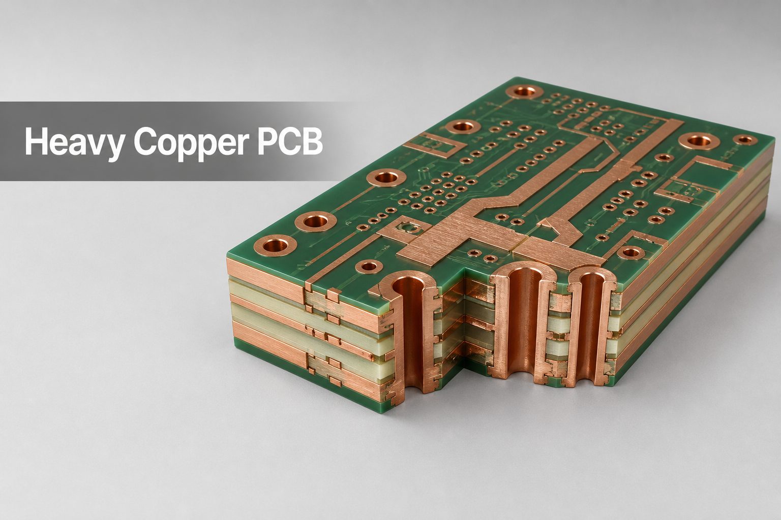
A heavy copper PCB is generally understood in the PCB industry as a rigid board with copper conductors of about 3 oz/ft² or more on one or more layers. The term is not a single IPC product class, so the fabrication drawing should state the finished copper thickness required on every layer instead of relying on the words “heavy copper” alone.
Higher pcb copper weight increases the conductor cross-section available for current and heat spreading, but it also changes etching, plating, lamination, drilling, solder-mask coverage, and assembly behavior. Typical applications include power distribution, motor drives, battery systems, power converters, planar magnetics, welding equipment, industrial controls, and high-current protection circuits.
What Copper Thickness Can EBest Circuit Support?
Our current FR-4 process matrix separates routine production from special-process review. Standard designs cover inner-layer copper from 0.5 to 5 oz and outer-layer copper from 1 to 5 oz. Copper from 5 to 20 oz is listed as a special process for both inner and outer layers.
| Layer position | Standard process | Special process | Quotation status |
| FR-4 inner layer | 0.5–5 oz | 5–20 oz | Confirm finished copper by layer |
| FR-4 outer layer | 1–5 oz | 5–20 oz | Confirm base foil plus plating |
| 20–200 oz extreme copper | Not a standard matrix range | Project-specific engineering review | Stackup, size, geometry and quantity required |
Our public product page describes extreme copper projects up to 200 oz. That figure should be treated as an engineering-review target, not a blanket promise that can be combined with every layer count, hole size, board dimension, material, or tolerance. A 100 oz+ request requires a dedicated feasibility review before the layout is frozen.
Which Heavy Copper PCB Stackups Are Typical?
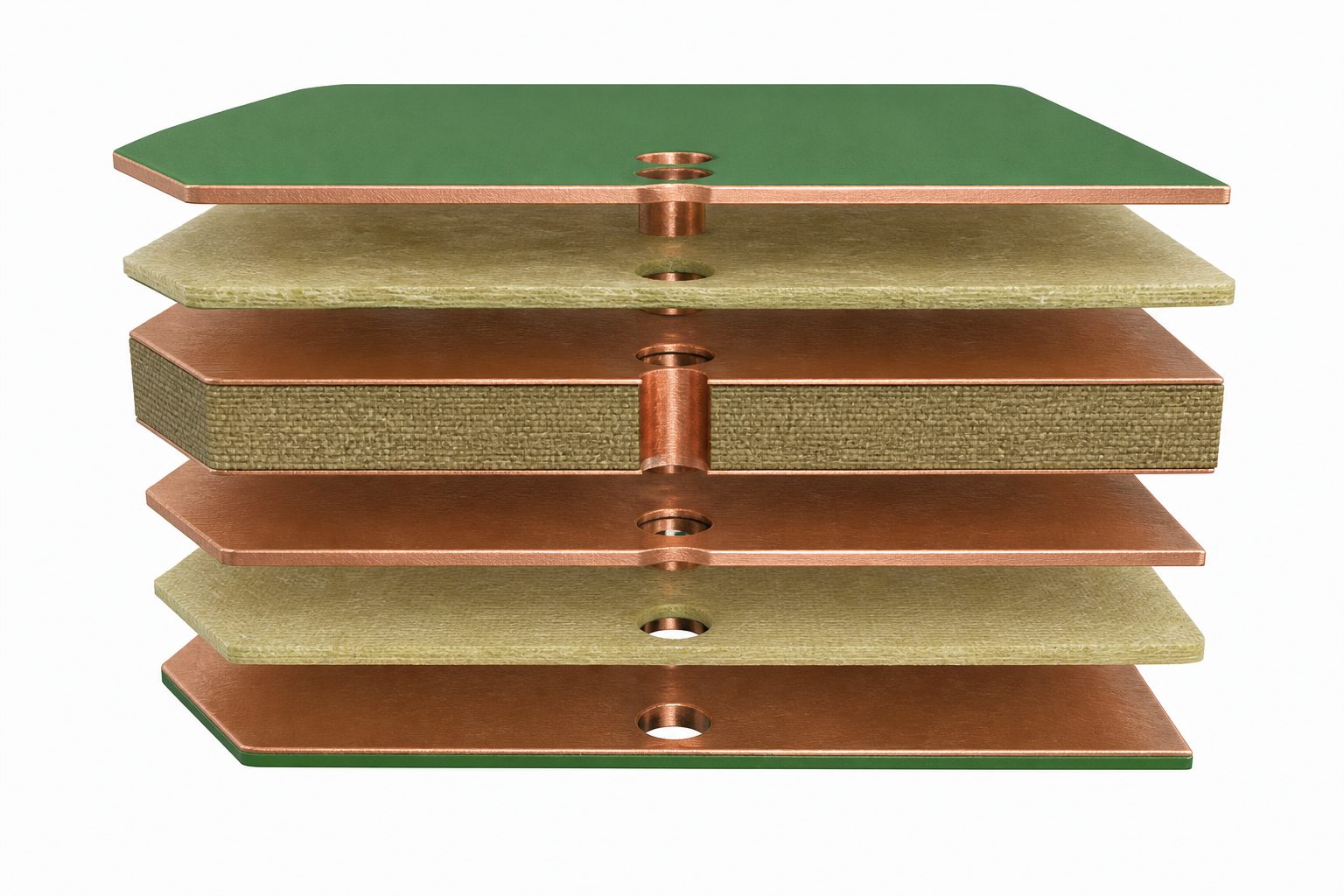
Typical stackups keep copper mass as balanced as the electrical design allows. The exact core and prepreg construction is selected after we review copper coverage, finished board thickness, current paths, isolation requirements, hole structures, and assembly constraints.
| Configuration | Typical use | Main DFM focus |
| Two-layer heavy copper | Simple high-current distribution and power conversion | Symmetric copper, isolation spacing and solderability |
| Four-layer balanced power board | Separate power, ground and control functions | Mirror copper weight and coverage around the centerline |
| Mixed-copper multilayer | Heavy power layers with lighter signal layers | Resin fill, lamination pressure, thickness control and registration |
| Extreme-copper custom construction | Very high-current terminals, switches or power modules | Fabrication route must be agreed before detailed layout |
For stable heavy copper PCB design, avoid placing most of the copper mass on only one side of the stack. Large differences in copper coverage can increase resin-flow difficulty, thickness variation, bow, and twist. We may request copper balancing or thieving changes that do not alter the electrical function.
Which Materials and Prepreg Systems Are Used?
FR-4 is the usual starting material, but the resin system must match the copper volume, thermal exposure, electrical requirements, and final board thickness. Our current material matrix includes low-, mid-, and high-Tg FR-4 options, with high-Tg material required for standard constructions of eight layers or more.
- Standard FR-4 prepregs: 1080, 2116 and 7628.
- High-Tg FR-4 examples: KB6167, ITEQ IT180, SY-S1170 and S1000-2.
- Special material options: selected Isola, Nelco, Rogers, Taconic, PTFE and halogen-free systems, subject to stackup and procurement review.
- Core selection: based on dielectric thickness, copper weight, required finished thickness and lamination filling demand.
Prepreg style alone does not guarantee a void-free heavy-copper build. Copper topography, remaining resin volume, pressure distribution, panel size, and copper coverage all affect fill. For deep conductor steps or 100 oz+ structures, we first review whether a conventional multilayer route is appropriate or whether a different conductor architecture is required.
Which Surface Finishes Are Available?
Available FR-4 surface finishes include OSP, HASL, ENIG, immersion silver, immersion tin, ENEPIG, hard gold fingers, and selected combined finishes. The correct option depends on pad flatness, shelf life, soldering process, contact wear, wire bonding requirements, and exposed-copper areas.
| Surface finish | Common selection reason | Heavy-copper review point |
| OSP | Simple solderable copper protection | Handling, multiple heat cycles and exposed-copper plan |
| HASL / lead-free HASL | Established solderable finish | Surface planarity and large thermal mass |
| ENIG | Flat pads and broad assembly compatibility | Nickel/gold coverage around high copper steps |
| Immersion silver or tin | Flat soldering surface | Storage, handling and process compatibility |
| ENEPIG | Soldering and selected wire-bonding applications | Confirm bonding method and finish specification |
| Hard gold fingers | Wear-resistant edge contacts | Gold thickness, bevel and selective plating area |
The finished board thickness range also varies with the selected finish. If your drawing combines thick copper with selective gold, exposed bus areas, press-fit holes, or large solder terminals, identify those regions clearly in the fabrication notes.
What Design Rules and Manufacturing Tolerances Apply?
Design rules become wider as copper thickness increases because the etching and plating window changes. Do not apply a 1 oz line/space rule to a 6, 10, or 20 oz layer. The values below are from our current FR-4 capability matrix and must still be checked against the full stackup.
| Finished copper | Inner standard line/space | Inner special line/space | Outer standard line/space | Outer special line/space |
| 2 oz | 6/6 mil | 5/5 mil | 8/8 mil | 6/6 mil |
| 3 oz | 10/12 mil | 8/8 mil | 12/12 mil | 9/9 mil |
| 4 oz | 12/16 mil | 10/10 mil | 16/16 mil | 12/12 mil |
| 5 oz | 16/20 mil | 10/14 mil | 20/20 mil | 15/15 mil |
| 6 oz | 22/26 mil | 14/16 mil | 26/26 mil | 20/20 mil |
| 10 oz | 36/40 mil | 28/34 mil | 40/40 mil | 32/32 mil |
| 20 oz | 74/90 mil | 60/80 mil | 90/90 mil | 70/70 mil |
General FR-4 drilling tolerances in the same matrix are ±3 mil for plated-hole diameter and ±2 mil for non-plated-hole diameter under the standard process, with tighter special-process values of ±2 mil and ±1 mil respectively. Outline tolerance is typically ±5 mil. These values are not automatically combinable with maximum copper, maximum thickness, minimum holes, maximum aspect ratio, and maximum board size in one design.
Use our heavy copper PCB design guide as an early reference, then send the actual files for DFM. For current-carrying calculations, IPC-2152 relates conductor size, current and acceptable temperature rise; it does not replace thermal simulation, terminal analysis, or prototype validation for the finished assembly.
Which Via Technologies Are Available?
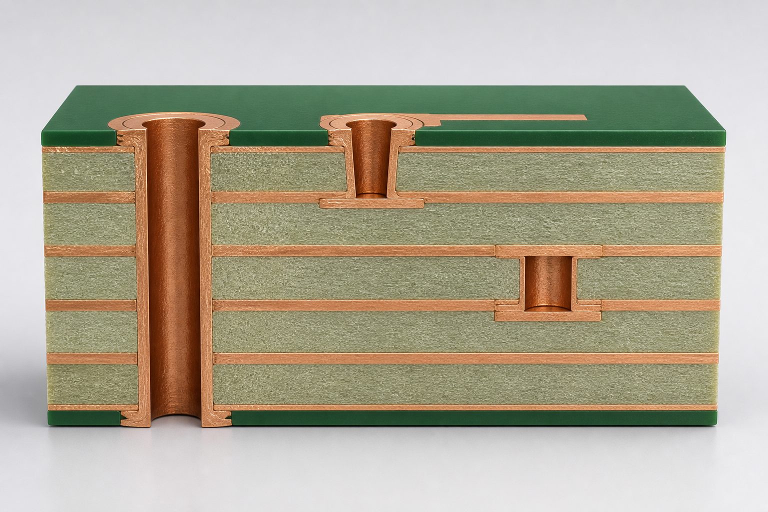
Through holes, mechanical blind/buried holes, and laser blind/buried vias are listed in our FR-4 capability matrix. The generic matrix shows 0.10 mm laser blind/buried vias, 0.20 mm standard mechanical blind/buried holes, and 0.15 mm special mechanical blind/buried holes.
- Plated through holes: standard maximum aspect ratio 8:1; special process up to 10:1.
- Mechanical blind/buried holes: 0.20 mm standard and 0.15 mm special-process minimums.
- Laser blind/buried vias: 0.10 mm listed capability for suitable HDI constructions.
- High-current transitions: multiple parallel vias, larger finished holes, thicker barrel copper, or direct copper structures may be considered after current and thermal review.
These minimums describe the broader FR-4 process range, not a guarantee that microvias can be combined with 20 oz or 100 oz copper. On heavy power layers, larger via structures and generous annular rings are usually more manufacturable. We confirm drill diameter, pad size, finished barrel copper, aspect ratio, and connection pattern together.
Which Standards and Certifications Apply?
The applicable document set depends on the product class, end market, customer drawing, and purchase specification. A heavy copper board should not be described as “IPC compliant” without naming the exact document, revision, class, and acceptance requirements.
- IPC-2152: guidance for determining current-carrying capacity from conductor size and acceptable temperature rise.
- IPC-2221 and IPC-2222: generic and rigid-board design requirements.
- IPC-6012F: qualification and performance requirements for rigid printed boards.
- IPC-A-600: acceptability criteria for printed boards when called out with the applicable performance specification.
EBest Circuit company materials list ISO 9001:2015, ISO 13485:2016, IATF 16949, AS9100D, UL, RoHS and REACH documentation. Certification scope is not identical for every product, manufacturing site, or end use. State your industry and required certificate package in the RFQ so we can confirm the applicable manufacturing route and provide the relevant evidence.
What Determines Typical Lead Time?
Heavy copper lead time is quoted after DFM because the work does not follow one standard prototype schedule. The public EBest Circuit lead-time table directs special boards to contact us for project-specific timing, and that is the correct approach for heavy and extreme copper.
- Finished copper weight on every inner and outer layer.
- Layer count, board thickness, panel size and copper balance.
- Laminate and prepreg availability, including special or halogen-free systems.
- Mechanical, blind, buried or laser-via requirements.
- Surface finish, selective plating and solder-mask build.
- Prototype quantity, production quantity and test-coupon requirements.
- DFM clarification cycles and customer approval time.
To shorten the schedule, submit a complete, internally consistent package and approve the proposed stackup before detailed routing is locked. You can review our general PCB lead-time framework, but the written quotation and order acknowledgement govern the actual heavy-copper delivery date.
How Should Engineers Design 100 oz+ PCBs?
A 100 oz+ board must be treated as an extreme copper PCB project, not as a 10 oz layout with every dimension multiplied. One ounce of copper per square foot is approximately 35 µm, so 100 oz represents roughly 3.5 mm of copper before considering dielectric layers, plating, surface finish, and fabrication tolerances.
- Define the electrical target. Provide continuous and peak current, duty cycle, allowed voltage drop, ambient conditions, cooling method and maximum temperature rise.
- Specify finished copper by layer. State which layers require 100 oz+ and whether the target includes plated build-up. Do not use one global copper note for a mixed construction.
- Separate power and signal needs. Keep fine-pitch control circuitry away from the extreme-copper geometry or place it on a separate assembly when practical.
- Use broad, simple conductors. Avoid fine neck-downs, dense spacing, small thermal spokes and abrupt current bottlenecks. Exact minimum geometry must come from project DFM.
- Minimize layer transitions. Where current must change layers, define the total current path through terminals, copper features and via structures rather than counting vias alone.
- Balance the construction. Keep copper mass and coverage as symmetric as possible to reduce lamination and flatness risk.
- Reserve mechanical space. Expect larger pads, holes, clearances, edge distances and finished board thickness than a normal PCB.
- Freeze the layout after fabricator DFM. We must agree on the manufacturing route, stackup, conductor geometry, tolerances, coupon plan and inspection criteria before release.
These are high current PCB design guidelines, not a released 100 oz design-rule table. EBest Circuit’s controlled FR-4 matrix currently provides numeric line/space rules through 20 oz. Any 100 oz+ geometry remains subject to engineering feasibility, material sourcing, panel constraints, and a written project-specific rule set.
What Should You Send for DFM Review and Quotation?
A complete package lets us distinguish a feasible heavy-copper build from a requirement that needs structural changes. Send the electrical requirements together with the fabrication data, not just Gerber files and a single copper number.
- Gerber or ODB++ data, NC drill files, drill table and board outline.
- Layer stackup with finished copper weight for every layer.
- Finished board thickness, tolerance, dimensions and quantity.
- Material family, Tg, CTI, flammability and halogen-free requirements where applicable.
- Surface finish, selective plating, exposed copper and edge-contact requirements.
- Continuous/peak current, temperature-rise limit, duty cycle and cooling conditions.
- Required IPC document, class, test coupons, microsections, electrical test and certificate package.
- Prototype target date and production forecast.
Our general PCB capability page provides broader reference data. For a binding decision, the reviewed stackup, DFM response and quotation take priority over standalone website maxima.

FAQ About Heavy Copper PCB
Is 3 oz copper considered heavy copper?
Many PCB manufacturers use 3 oz/ft² as the practical starting point for heavy copper, although there is no single IPC definition that makes the label sufficient for fabrication. Always state the finished copper thickness required on each layer.
Can inner and outer layers use different copper weights?
Yes. Mixed-copper stackups can place heavier copper on power layers and lighter copper on signal layers. The combination must be reviewed for resin fill, copper balance, finished thickness, registration and the line/space required on each layer.
Can heavy copper PCBs use blind or buried vias?
They can in suitable constructions, but the smallest generic FR-4 via capability cannot automatically be combined with the highest copper weight. We review hole type, connection layers, annular ring, dielectric thickness and copper build together.
Does thicker copper always allow more current?
Thicker copper increases conductor cross-section, but current capacity also depends on trace width, temperature-rise limit, adjacent copper, board material, airflow, enclosure, duty cycle, terminals and layer position. Use IPC-2152 as a design reference and validate the complete assembly.
Which finish is best for a heavy copper power board?
There is no universal finish. ENIG is useful where pad flatness matters, HASL is an established solderable option, OSP is simple, and ENEPIG may support selected bonding needs. The assembly process, storage plan, contact wear and selective-plating requirements decide the finish.
Can EBest Circuit make a 100 oz PCB?
We evaluate 100 oz+ requests as extreme-copper projects. Our controlled FR-4 matrix provides standard and special rules through 20 oz, while higher public maxima require project-specific confirmation. Send the stackup, geometry, current target, board size and quantity for a written feasibility decision.
How Can EBest Circuit Support Your Heavy Copper PCB Project?
At EBest Circuit, we support heavy copper PCB stackup review, material selection, DFM, prototype fabrication, production planning, electrical testing and cross-section inspection. We will identify which requirements fit the standard process, which require a special route, and which need redesign before they become cost or reliability problems.
Send your files and operating requirements through our PCB quotation and engineering contact page. For 20 oz, 100 oz+ or mixed-copper multilayer designs, request the project-specific stackup and design rules before final layout release.
You may also like








Tags: Extreme Copper PCB, heavy copper pcb design, Heavy copper PCB manufacturer, High Current PCB Design Guidelines, PCB Copper Weight