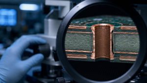
PCB microsection analysis is a destructive inspection method that cuts through a board or test coupon, mounts the sample, grinds and polishes it, then examines the exposed structure under a microscope. It can show plating distribution, via-wall cracks, inner-layer connections, registration, laminate condition and other internal features that remain hidden during ordinary visual inspection.
The method is powerful, but a polished image alone is not a verdict. A useful result depends on representative sampling, correct preparation, a known inspection plane and acceptance criteria tied to the applicable drawing, procurement specification and product class. This guide explains how to plan the analysis, read the evidence and turn the report into a manufacturing decision.
What PCB Microsection Analysis Actually Shows
A microsection provides a direct two-dimensional view through selected internal PCB features. It is commonly used to evaluate plated through-holes, blind or buried vias, copper interfaces, laminate layers and selected solder joints. Because the sample is physically cut, the analyst can inspect material boundaries rather than infer them from an external image.
The method is especially useful when the question is structural: Is the hole wall continuous? Does the plated copper connect cleanly to the inner layer? Is there evidence of resin recession, separation, cracking or voiding? Are layers aligned around the inspected feature? These questions are different from verifying the electrical netlist, so microsection results should complement—not replace—appropriate electrical and functional tests.
| Feature | What the section can reveal | Decision supported |
| Plated hole or via barrel | Continuity, local thin areas, cracks, nodules or voids | Plating-process and thermal-reliability review |
| Inner-layer connection | Land contact, resin smear evidence, separation or breakout | Drilling, desmear and registration review |
| Multilayer stack | Layer position, dielectric condition and local registration | Lamination and imaging-process review |
| Surface and hole finish | Local layer interfaces and coating condition | Finish-process investigation |
| Solder joint | Internal wetting profile, voids, cracks and interface condition | Assembly failure analysis |
When a Microsection Is Worth the Destructive Sample
Use microsectioning when direct internal evidence is more valuable than preserving the selected sample. Good triggers include process qualification, lot acceptance required by contract, investigation of a suspected via or interconnect failure, validation after thermal stress, and confirmation that a corrective action changed the internal result.
Do not order a section merely because it appears thorough. Start with the failure question. If the issue is an open circuit, an electrical test can locate the affected net before cutting. If the concern is a hidden BGA solder joint, X-ray may narrow the location. If the concern is hole-wall plating or an inner-layer interface, cross-sectioning may provide the decisive evidence.
For an overview of where microsection preparation sits among other procedures, review the IPC-TM-650 PCB test methods guide. The applicable test method defines preparation or measurement practice; the purchase drawing and product specification still need to define what is acceptable for the actual board.
Coupon or Production Board: Choose the Sample Before Cutting
The sample must represent the process and the feature under investigation, or the microscope image can answer the wrong question with great precision. A production coupon avoids sacrificing a sellable board and can be designed around representative holes, traces and layer relationships. A failed production board may be necessary when the investigation concerns one specific field failure or localized anomaly.
Record the panel position, lot, board revision, coupon identity, target hole or via, prior thermal exposure and cutting orientation before preparation. For intermittent failures, first preserve photographs and electrical evidence. Once the sample is cut and polished, the original condition cannot be reconstructed.
- Use a defined coupon when the goal is routine process monitoring or contractual conformance.
- Use the affected board when location-specific evidence is essential and the sample can be sacrificed.
- Use more than one location when the suspected problem could vary across a panel or stackup.
- Keep an unsectioned control sample when comparison may be needed later.
How the Microsection Preparation Process Works
The usual sequence is target selection, sample removal, mounting, controlled grinding, fine polishing, optional micro-etching and microscopic examination. Each step can change the surface, which is why preparation quality must be checked before interpreting a defect.
- Define the target plane. Mark the exact hole, via, interface or joint and the direction of the intended cut.
- Remove the specimen. Leave enough material around the target to avoid mechanical damage at the feature of interest.
- Mount the sample. Encapsulate and support the specimen so dissimilar materials remain stable during grinding.
- Approach the target gradually. Coarse removal gets near the inspection plane; finer abrasives reduce deformation and deep scratches.
- Polish the exposed face. The final surface must be clear enough to distinguish copper, resin, glass reinforcement and interfaces.
- Apply micro-etch only when justified. Etching can improve contrast, but excessive etching may alter the apparent boundary.
- Capture calibrated images. Record magnification, scale, target identity and measurement locations.
IPC-9241 discusses variables and problems across this preparation chain. It is a valuable process reference, but it does not eliminate the need for a product-specific acceptance plan.
What to Measure Around Plated Through-Holes and Vias
Measure the features that connect directly to the suspected risk, not every visible dimension by habit. For plated holes and vias, the inspection plan may include local copper distribution, barrel condition, the inner-layer connection, annular relationship, dielectric separation and evidence of cracking or voiding.
Measurements must identify where they were taken. A single favorable point can hide a local thin area, while an off-center section can make the geometry look misleading. The report should show the complete inspected feature plus higher-magnification images of relevant interfaces.
Annular geometry is easier to interpret when the design intent is already understood. The related guide on annular rings in PCB design explains the relationship between the finished hole, pad and registration allowance.
How Microsections Reveal Lamination and Registration Problems
A well-targeted section can show whether internal layers and dielectric interfaces are positioned and bonded as expected at that location. The analyst may see local layer shift, uneven dielectric spacing, separation, resin-rich or resin-starved areas, disturbed glass bundles or damage near drilled features.
Interpret these observations in context. A cross-section is a narrow plane through a three-dimensional product. One local observation does not automatically describe the entire panel, and a visual difference is not automatically a reject. Correlate the image with panel position, stackup, drilling route, lamination history and the specified acceptance criteria.
HDI constructions deserve special attention because sequential lamination and microvia structures create multiple interfaces. For a wider process view, see the HDI PCB manufacturing process guide.
Which Defects Are Real and Which Are Preparation Artifacts
Scratches, edge rounding, copper smearing, pull-out, excessive etch and a section that misses the target center can imitate or conceal real defects. Before declaring a crack or void, check whether the feature continues consistently, whether adjacent material is distorted and whether a second preparation or viewing condition confirms it.
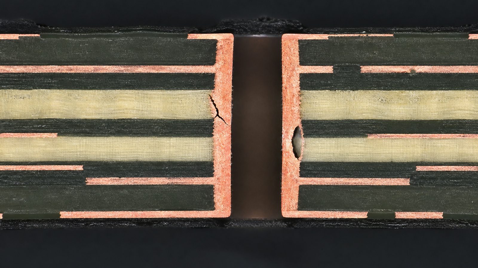
A disciplined report separates three statements: what is visibly observed, what criterion applies and what root-cause hypothesis remains to be tested. For example, “a discontinuity is visible at the knee” is an observation. “The feature does not meet drawing requirement X” is an acceptance conclusion. “Thermal stress caused the discontinuity” is a causal hypothesis that may require history, replication or additional analysis.
Microsection vs X-Ray, AOI and Electrical Test
No single inspection method covers all PCB risks; choose the method according to the physical question. Cross-sectioning gives direct material and interface evidence at one destroyed location. X-ray shows density and geometry without cutting. AOI evaluates visible surfaces. Electrical test verifies connectivity and isolation but does not explain every structural cause.
| Method | Best question | Main limitation |
| Microsection | What is happening inside this material interface? | Destructive and highly location-dependent |
| X-ray | Is hidden geometry, voiding or alignment suspicious? | Overlapping features and material density can limit interpretation |
| AOI / visual inspection | Are visible surfaces, patterns or components acceptable? | Cannot directly see most internal interfaces |
| Electrical test | Are intended connections present and unintended connections absent? | May not reveal a structurally weak connection that still conducts |
| Functional test | Does the assembled product perform its intended function? | May locate the symptom without isolating the physical cause |
A broader method-selection comparison is available in the PCB testing methods and equipment guide.
How to Read a PCB Microsection Report
A decision-ready report must connect every image and measurement to a traceable sample, target feature and acceptance requirement. Attractive microscope photographs without identification, scale or disposition are not enough for lot release or corrective action.
- Confirm the purchase order, board number, revision, lot and sample identity.
- Verify whether the sample is a coupon or production board and where it came from on the panel.
- Check preparation orientation and whether the inspected plane passes through the intended feature.
- Require a scale bar or calibrated measurement reference on measurement images.
- Match each reported value to a clearly marked location.
- Separate observations from acceptance decisions and root-cause hypotheses.
- Identify the drawing, specification revision and product class used for disposition.
- Record whether thermal conditioning or other preconditioning occurred before sectioning.
- Ask for a clear Pass, Fail or Engineering Review disposition with the reason.
How to Write Acceptance Criteria Into the PO and Quality Plan
Specify the governing documents, product class, coupon plan, sampling trigger, inspected features and required report content before fabrication starts. A late request for “a microsection report” can produce images that do not answer the buyer’s actual reliability concern.
Do not copy a generic numerical limit into every project. Acceptance depends on board technology, applicable IPC performance specification, customer drawing, qualification status and contract. State which document controls if requirements conflict. Also define whether a failed coupon stops the lot, triggers additional samples or requires an engineering review.
A practical PO note can request: board and lot traceability; coupon identity and panel location; specified preconditioning; defined inspection features; calibrated images; the applicable requirement beside each result; and retention of the report for an agreed period.
What to Send for a Failure-Analysis Review
Send enough evidence to preserve the failure context before anyone chooses the cut location. The most useful package includes the board revision, Gerber or ODB++ data, stackup, fabrication notes, drill information, affected net or component, symptoms, electrical measurements, thermal history, lot data and marked photographs of the suspect location.
If assembly is involved, add the BOM, CPL, assembly drawing, reflow history when available and the exact point at which the failure appeared. State whether the goal is conformance verification, root-cause investigation or process comparison; each goal may require a different sample plan.
Never cut the only failed sample before documenting it. When the defect may be intermittent, preserve electrical behavior and external condition first. The sectioning plan should be approved by the person responsible for the investigation.
How Microsection Findings Should Change Production Controls
The value of microsection analysis comes from the control change it supports, not from the microscope image itself. A confirmed issue should be traced to the relevant process window—such as drilling, desmear, plating, lamination, imaging, thermal exposure or assembly—and linked to containment, root-cause verification and corrective action.
For recurring production, compare like-for-like evidence: the same coupon design, target feature, preparation orientation, measurement definition and acceptance rule. Otherwise, apparent improvement may be caused by a changed inspection method rather than a changed process.
- Contain suspect lots and protect traceability.
- Confirm the observation with suitable repeat evidence.
- Identify the process variable capable of producing that structure.
- Change and document the control or process window.
- Verify effectiveness with new representative samples.
- Update the control plan, work instruction or supplier requirement.
FAQ About PCB Microsection Analysis
Is PCB microsection analysis destructive?
Yes. The selected coupon or board area is cut, mounted, ground and polished. Use a production coupon when possible, and document any unique failed sample before sectioning because the original condition cannot be restored.
Is microsectioning the same as cross-section analysis?
In PCB work, the terms are commonly used for the same preparation-and-inspection approach. “Microsectioning” emphasizes specimen preparation, while “cross-section analysis” emphasizes examination and measurement of the exposed plane.
Can a microsection prove that the whole PCB lot is good?
Not by itself. It directly represents the inspected sample and plane. Lot conclusions require an agreed coupon design, sampling plan, panel-location logic and acceptance rule that make the evidence representative.
Can X-ray replace PCB microsection analysis?
Not for every question. X-ray is non-destructive and useful for hidden geometry and density differences, while a microsection directly exposes material interfaces. The two methods often complement each other during failure analysis.
What standards are commonly associated with PCB microsections?
IPC-9241 addresses microsection preparation guidance, and IPC-TM-650 includes relevant preparation and dimensional inspection methods. Product acceptance normally comes from the applicable performance specification, acceptability standard, drawing and purchase requirements.
Should a coupon be thermally stressed before sectioning?
Only when the qualification or investigation plan requires it. Preconditioning can expose weaknesses that are not visible in an as-received sample, but the condition, cycle and sequence must be recorded so results remain interpretable.
What makes a microsection report traceable?
It should identify the board, revision, lot, coupon or sample, panel location when relevant, target feature, preparation orientation, image scale, measurement locations, governing requirements and final disposition.
Why can two laboratories report different measurements?
Differences may come from sample position, section plane, edge preparation, calibration, measurement definition or interpretation. A shared method, marked measurement locations and retained images make comparisons more reliable.
How do I avoid confusing an artifact with a real crack?
Check preparation quality, nearby material deformation and whether the feature persists under another viewing condition or repeat section. A real defect conclusion should not rely on one ambiguous image.
What files should accompany an RFQ that needs microsection evidence?
Send Gerber or ODB++, stackup, drill data, fabrication drawing, board class or performance requirement, coupon or sampling expectations, required preconditioning, inspection features, report format, quantity and target schedule.
Turn the Cross-Section Into a Clear Manufacturing Decision
A good microsection plan starts before cutting: define the risk, choose a representative target, control preparation and connect every observation to an agreed acceptance rule. That discipline prevents both false rejects and false confidence.
Need a PCB or PCBA quotation with defined cross-section evidence? Send EBest Circuit your Gerber or ODB++ files, stackup, drill data, quantities, product class, coupon or sampling expectation, preconditioning requirement and target delivery date. Our engineering team can review the manufacturing package and clarify which inspection evidence should be included before production. Email sales@bestpcbs.com to request a DFM and quality-plan review.