






AI PCB design tools can help create circuits, suggest parts, place components, route traces, explain rule violations, and review documentation—but they do not make an unverified layout safe to fabricate. Their best use is to shorten bounded tasks inside a controlled engineering workflow. Requirements, constraints, simulation, DRC, DFM review, and final release approval still need accountable human judgment.
This guide separates useful automation from risky overconfidence. It compares tool roles, identifies decisions that remain engineering work, and provides a release checklist you can use before sending AI-assisted PCB files to a manufacturer.
Can your team prove that the AI-generated board matches the product—not merely that the CAD file opens?
A plausible-looking layout can still contain the wrong footprint revision, a weak return path, unreviewed impedance geometry, inaccessible test points, a copper-to-edge problem, incomplete drill notes, or manufacturing rules copied from the wrong supplier. Those errors become expensive when they survive until fabrication, assembly, or first power-on.
EBest Circuit can review the released manufacturing package against the actual board construction and requested production scope.
Send Gerber or ODB++, NC drill files, fabrication drawing, stackup, material and copper requirements, controlled-impedance notes, netlist or IPC-356 data where available, quantity, surface finish, test requirements, and target delivery. For assembly, also include the BOM, CPL/pick-and-place file, assembly drawings, approved substitutions, and programming or test instructions. Project-specific capability and special-process requirements are confirmed during review rather than inferred from an AI prompt.
Can AI Design a PCB From Schematic to Gerbers?
AI can participate across the workflow, but “design a PCB” covers several different engineering jobs. A text request may produce a circuit concept or first-pass schematic. A placement engine may optimize component locations against encoded goals. An autorouter may complete connections under a defined rule set. A review assistant may explain a DRC finding. None of these steps proves the full product requirement.
The important question is not whether a tool can generate output. It is whether the input constraints are complete and whether the output can be independently verified. A correct netlist does not prove signal integrity. A DRC-clean layout does not prove that the selected rules match the chosen stackup. Generated Gerbers do not prove that drill pairs, impedance callouts, materials, tolerances, assembly clearances, and test access are complete.
For that reason, treat AI output as a candidate design state. A qualified engineer should still approve the circuit, part choices, footprint library, placement, critical routing, power integrity, thermal path, manufacturability, testability, and final release package.
AI PCB Design Tools by Job: Schematic, Placement, Routing and Review
Choose an AI PCB design tool by the task it performs and the evidence you need from that task. “AI-powered” is not a useful comparison unless the buyer knows what enters the system, what it changes, which constraints it honors, and how a human can inspect or override the result.
| Tool or approach | Useful role | Input that must be controlled | Engineer must still verify |
|---|---|---|---|
| Flux | Browser-based schematic and PCB collaboration with an AI assistant and layout automation | Requirements, approved parts, schematic intent, placement constraints, routing rules, stackup assumptions | Footprints, critical nets, physical layout, rule completeness, DFM package |
| Quilter | Physics-driven placement and routing from a supplied circuit design and constraints | Validated circuit, board outline, constraints, component data, design priorities | Whether the completed layout meets product, SI/PI, thermal, test, and manufacturing needs |
| Cadence Allegro X AI | Generative assistance for placement and routing inside a professional PCB environment | Constraint system, technology files, library quality, layer strategy, critical-net definitions | Constraint accuracy, routing quality, signoff analyses, release data |
| Zuken CR-8000 AIPR | Intelligent place-and-route informed by design libraries and established design practices | Reusable design knowledge, validated rules, board architecture, technology setup | Project-specific exceptions, performance, manufacturability, final approval |
Product functions, licensing, deployment, supported formats, and data-handling terms change. Verify the current version and security model before uploading confidential schematics, component data, or product requirements. Also distinguish a circuit-generation assistant from an autonomous layout system and from conventional rule-based autorouting; their risks and required reviews are not the same.
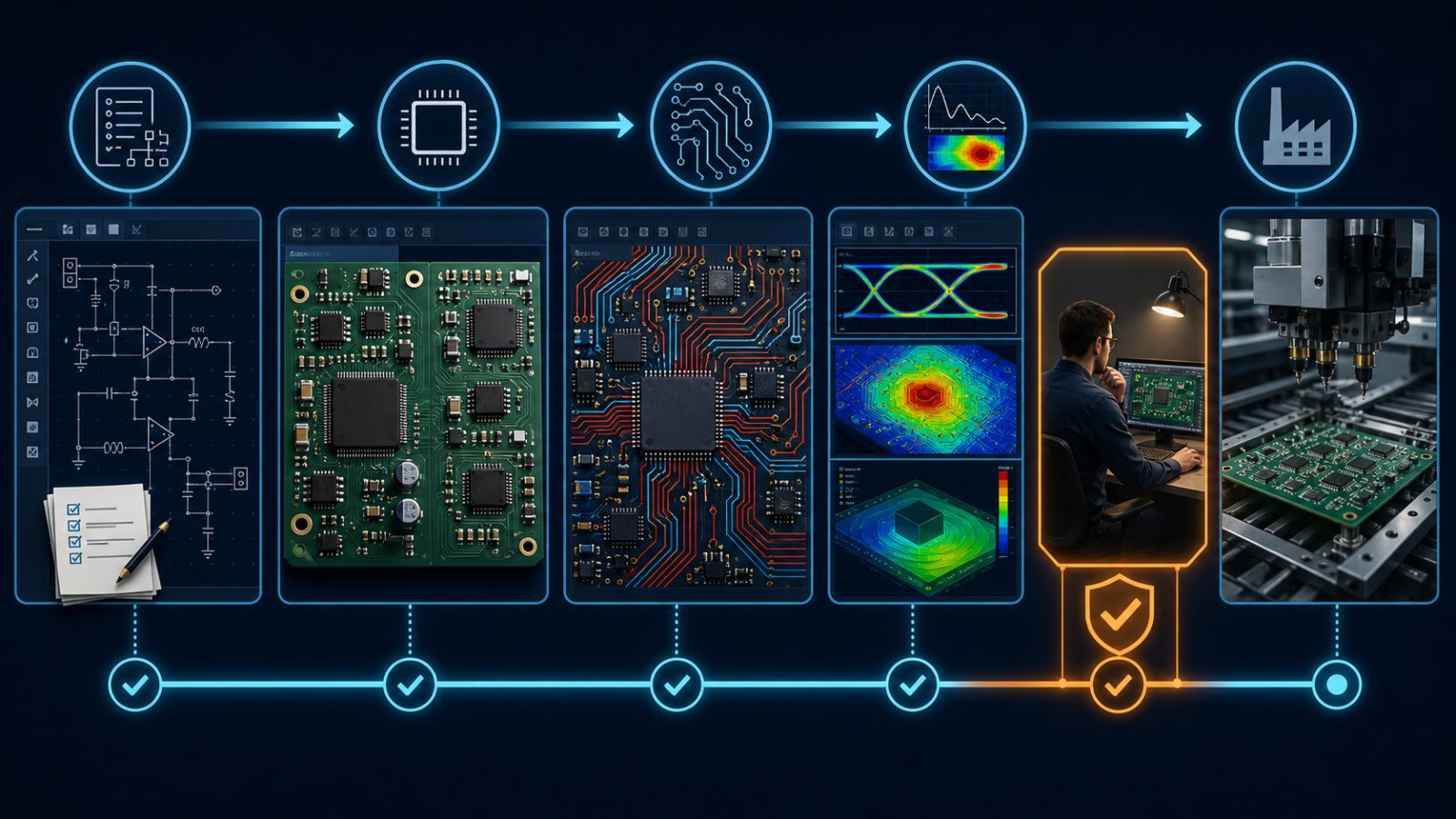
Where AI PCB Layout Still Needs Engineer Judgment
The hardest layout decisions are often interactions, not isolated rules. Moving a connector may improve enclosure fit but worsen an ESD path. Spreading components may improve assembly access but enlarge a sensitive current loop. Adding copper may help current capacity while changing thermal balance or impedance. AI can search alternatives, but an engineer must decide which tradeoff serves the product.
- Architecture and safety: isolation boundaries, creepage, clearance, protection devices, grounding concept, and applicable product standards.
- Signal and power integrity: reference-plane continuity, return-current paths, impedance geometry, crosstalk, differential-pair behavior, decoupling, and power-distribution impedance.
- Thermal behavior: component loss, heat spreading, copper balance, thermal vias, airflow, enclosure conditions, and temperature-sensitive parts.
- RF and analog behavior: placement sensitivity, shielding, guard structures, antenna keep-outs, matching networks, noise coupling, and tuning access.
- Mechanical integration: enclosure tolerances, connector alignment, mounting hardware, rigid-flex bend areas, cable access, and assembly sequence.
- Manufacturing and test: realistic line/space and hole choices, annular rings, solder-mask geometry, assembly clearances, panel strategy, fiducials, tooling, probing, inspection access, and rework risk.
These decisions also depend on the selected manufacturer’s verified process window. For example, line/space, finished-hole size, aspect ratio, copper weight, material, layer count, and blind/buried-via construction are linked constraints. A value that is routine for one construction may require special review for another. Do not let an AI tool turn a generic rule table into an unconditional fabrication claim.
A Practical AI PCB Design Workflow From Requirements to Release Files
A safe workflow gives AI a narrow job, defines an observable acceptance test, and preserves a human approval gate. Use the following sequence whether the tool assists schematic creation, placement, routing, analysis, or documentation.
- Freeze the design brief. Record electrical requirements, interfaces, environment, dimensions, connector locations, compliance needs, test strategy, cost target, quantity, and lifecycle expectations.
- Control the component and footprint source. Approve manufacturer part numbers, lifecycle status, ratings, package variants, land patterns, 3D models, pin mapping, and substitution policy. Never accept a generated footprint on appearance alone.
- Validate the schematic. Review power sequencing, protection, pull states, unused pins, current paths, tolerance stack-ups, net naming, ERC results, and design calculations. Simulate critical behavior where appropriate.
- Define the physical technology. Establish board outline, stackup, copper weights, impedance needs, via strategy, fabrication classes, assembly process, and manufacturer rules before layout automation begins.
- Encode constraints by intent. Mark safety regions, high-current paths, high-speed classes, differential pairs, length relationships, return references, keep-outs, placement groups, thermal needs, and test access.
- Run AI or automation on a controlled revision. Preserve the input revision, tool version, settings, constraint files, generated output, warnings, and rejected alternatives. This creates a reviewable change instead of an unexplained new baseline.
- Review by risk, not by visual neatness. Inspect safety and power first, then clocks and high-speed interfaces, analog/RF regions, thermal paths, mechanical fit, manufacturability, and testability.
- Perform independent checks. Run ERC/DRC, connectivity comparison, field-solvers or SI/PI analysis where needed, thermal assessment, 3D/mechanical review, and a manufacturer-aligned DFM check.
- Generate and compare release files. Inspect Gerber/ODB++, drills, netlist, drawings, stackup, pick-and-place, BOM, and assembly outputs in viewers independent of the source editor.
- Obtain accountable signoff. Identify the engineer approving the circuit, layout, analyses, DFM exceptions, and released revision. An AI conversation is not an approval record.
If your team needs a manufacturing-focused review structure, use this PCB design for manufacturability checklist to connect CAD decisions to fabrication and assembly risks.
Move from an AI-generated layout to a reviewable manufacturing package.
Email Gerber or ODB++, NC drill, fabrication drawing, stackup, material and copper requirements, impedance notes, netlist data, quantity, finish, test scope, and target delivery. Add BOM, CPL, assembly drawings, and approved substitutions when assembly is required. EBest Circuit can review open manufacturing inputs and confirm the project-specific scope.
Gerber/ODB++ | Drills | Stackup | Drawing | Netlist | BOM/CPL | Quantity
12 Checks Before You Trust an AI-Generated PCB Layout
Use this list as a release gate, not as a late visual review. Each item should produce evidence that another engineer can inspect.
- Schematic-to-layout connectivity: compare the released netlist and confirm intentional net ties, no-connects, swapped pins, and variant handling.
- Library integrity: verify symbol-to-footprint mapping, pad numbering, polarity, courtyard, assembly origin, paste openings, and package revision.
- Power entry and protection: inspect current paths, fusing, reverse-polarity protection, surge/ESD parts, sequencing, and fault behavior.
- Return paths: trace the reference plane beneath critical signals and inspect every layer transition for a controlled return path.
- Impedance and timing: connect stackup geometry to the routed widths, gaps, layers, via structures, length relationships, and simulation assumptions.
- Spacing by voltage and environment: verify creepage, clearance, slots, coating assumptions, pollution conditions, altitude, and standard-specific requirements.
- Thermal path: review loss estimates, junction limits, thermal vias, copper spreading, heat-sink interfaces, airflow, and neighboring heat sources.
- Mechanical fit: compare board, connectors, fasteners, components, keep-outs, cables, and enclosure using the controlled mechanical model.
- Fabrication feasibility: check line/space, annular ring, drills, aspect ratio, copper balance, mask dams, board edge clearances, via fill/cap needs, and special processes against the actual construction.
- Assembly access: verify polarity visibility, component spacing, paste design, fiducials, tooling, selective-solder needs, inspection views, and rework access.
- Test strategy: confirm accessible test points, programming interface, power-up controls, isolation needs, fixture constraints, golden-unit plan, and measurement limits.
- Release consistency: ensure the revision, Gerbers/ODB++, drills, drawings, stackup, BOM, CPL, assembly notes, and change log describe the same build.
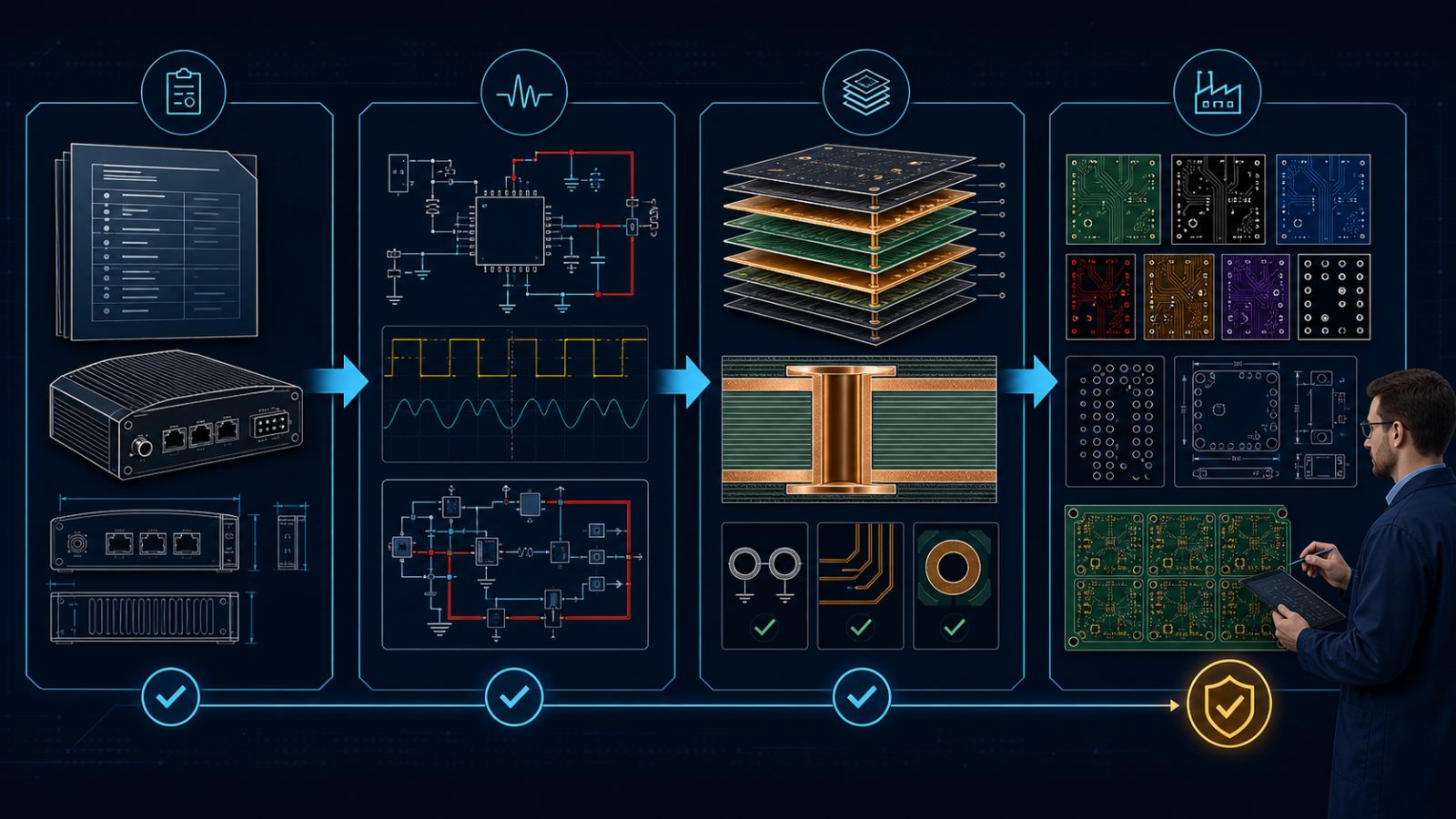
When AI Saves Time—and When Manual Layout Is Safer
AI is most useful when success can be expressed as constraints and checked independently. It can accelerate repetitive placement exploration, low-risk routing, component research, documentation, rule explanation, design comparison, and first-pass review. It can also help a small team expose missing questions earlier.
Manual or tightly supervised work is safer when the board contains safety-critical isolation, RF tuning, dense high-speed interfaces, mixed-signal sensitivity, unusual power conversion, extreme thermal conditions, novel packages, complex HDI structures, rigid-flex mechanics, or certification-sensitive requirements. These projects may still use AI, but the automation should not own the critical decision.
| Situation | Recommended AI role | Release condition |
|---|---|---|
| Simple controller or adapter with mature interfaces | Generate options, assist placement/routing, explain checks | Independent schematic, layout, DRC, DFM, and output review |
| Cost or area exploration | Compare constrained alternatives | Engineer documents the accepted tradeoff and downstream effects |
| High-speed, RF, precision analog, or power-dense board | Support analysis and bounded optimization | Domain specialist approves architecture, models, layout, and measurements |
| Safety- or compliance-sensitive product | Assist documentation and rule discovery | Applicable standards and responsible engineer govern every signoff |
| Prototype intended to become production | Accelerate early iterations without weakening records | Production stackup, test, panel, component, and process constraints are revalidated |
Speed is valuable only when the team can explain what was automated, what was checked, and what remains uncertain. If the verification cost approaches the cost of doing the critical work manually, automation may not be the faster path.
What Files Should Go to the PCB Manufacturer for DFM Review?
Send outputs that define the board, plus the assumptions needed to interpret them. A screenshot, AI transcript, or native CAD file alone is not a manufacturing package.
- Gerber X2, Gerber RS-274X, or ODB++ data that matches the released revision;
- NC drill and route data, including plated/non-plated definition and blind/buried-via pairs where applicable;
- fabrication drawing with board dimensions, tolerances, finished thickness, copper, material, finish, edge treatment, special notes, and revision;
- proposed stackup and controlled-impedance requirements, including target, tolerance, layer, reference, and coupon expectations;
- IPC-356 or another suitable netlist for an independent connectivity comparison where available;
- quantity, panel or delivery preferences, testing requirements, quality documentation, and target schedule;
- for assembly: BOM with approved manufacturer part numbers, CPL/pick-and-place data, assembly drawing, polarity notes, variant rules, programming, and test instructions.
Use a structured prototype PCB manufacturing RFQ checklist for early builds, then confirm that the same package can scale into repeat production. If supplier selection is still open, this PCB fabrication manufacturer selection guide explains how to compare capability evidence, engineering review, and quote assumptions.
How EBest Circuit Reviews AI-Assisted PCB Files Before Fabrication
The review starts with the released files and the intended construction—not with an assumption that an AI-designed board is either automatically good or automatically risky. The useful question is whether the package can be built, inspected, tested, and traced under an agreed scope.
EBest Circuit can check open manufacturing inputs such as layer definition, outline, drill data, annular features, spacing, copper-to-edge conditions, mask and legend interactions, stackup information, impedance notes, material and finish, panel considerations, fabrication drawings, and file consistency. For assembly projects, the review can extend to BOM/CPL alignment, polarity, package and footprint risks, assembly access, programming, and test inputs.
Capability values are confirmed against the actual construction. Standard and special-process ranges are not interchangeable, and combinations of minimum features, copper, thickness, materials, via structures, tolerances, and delivery needs require project review. For conventional FR-4 work, see the FR-4 PCB manufacturing overview; for microvia and high-density work, use the HDI PCB capability page as a starting point and submit the real stackup for confirmation.
If assembly is part of the build, include all controlled procurement and placement data so the fabrication and PCBA reviews describe one product. The custom PCB assembly guide shows how BOM, CPL, approved substitutions, inspection, programming, and testing affect the quote.
FAQ About AI PCB Design
Can AI design a complete PCB?
AI can generate or automate parts of the schematic and layout workflow, and some systems can complete placement and routing from supplied design data and constraints. A complete product still needs verified requirements, libraries, analyses, manufacturing rules, output checks, and accountable engineering approval.
Which AI tool is best for PCB design?
The best choice depends on the job. A schematic assistant, autonomous layout engine, professional place-and-route feature, and review assistant solve different problems. Compare supported formats, constraint depth, output inspectability, collaboration, IP controls, toolchain compatibility, and the amount of expert review required.
Can AI generate a PCB from a schematic?
Some tools can create placement and routing from a validated schematic or netlist plus board and routing constraints. The schematic alone is not enough: stackup, board outline, component locations, interfaces, power and signal classes, keep-outs, thermal needs, mechanical limits, manufacturing rules, and test access also matter.
Will AI replace PCB designers?
AI is more likely to change how designers explore, route, document, and review boards than to remove responsibility for product decisions. Engineers remain necessary for architecture, tradeoffs, constraint definition, analysis, safety, manufacturability, failure learning, and release signoff.
Can I use an AI-generated PCB layout for production?
Yes, if it passes the same engineering and manufacturing gates required for any production layout. Verify electrical behavior, libraries, signal/power integrity, thermal and mechanical performance, DRC, DFM, testability, output consistency, and revision control before release.
Is a DRC-clean AI layout ready to fabricate?
No. DRC only checks the rules that were encoded. It cannot prove that the rules match the selected stackup, manufacturer, product standard, assembly process, mechanical design, test strategy, or real operating environment.
What should I send for a DFM review of an AI-assisted board?
Send Gerber or ODB++, NC drills, fabrication drawing, stackup, material and copper requirements, impedance notes, netlist data where available, quantity, finish, testing needs, and target delivery. Add BOM, CPL, assembly drawings, substitutions, programming, and test instructions for PCBA.
Give the generated layout a manufacturing reality check before you release it.
Send the controlled PCB package and identify any AI-assisted stages, unresolved warnings, special constructions, impedance targets, or assembly needs. EBest Circuit will review the available fabrication and assembly inputs and confirm the build-specific quotation scope.
PCB Data | Stackup | Drawing | Netlist | BOM/CPL | Test | Schedule
You may also like






Tags: design for manufacturing, pcb design, pcb manufacturing