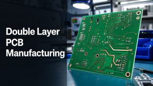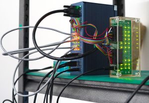
Double layer PCB manufacturing builds a circuit board with copper circuitry on both sides of an insulating core, connected by plated through holes when signals or power must pass from one side to the other. It is one of the most common PCB structures because it gives more routing space than a single-sided board while staying simpler and lower cost than multilayer PCB fabrication.
This guide is written for engineers, buyers, and product teams comparing two-layer PCB options for prototypes, control boards, power interfaces, LED boards, sensor modules, and general electronics. It explains the manufacturing process, design checks, cost factors, testing points, and RFQ files a supplier needs before quoting or building the board.
Double Layer PCB Manufacturing at a Glance
A double layer PCB uses top and bottom copper layers, normally with plated vias or through holes to connect the two sides. The buyer should confirm board material, copper weight, drill requirements, surface finish, solder mask, electrical testing, and assembly needs before approving production.
| Manufacturing area | What to confirm | Why it matters |
|---|---|---|
| Structure | Two copper layers, core material, board thickness and copper weight | Defines routing space, stiffness, cost and thermal behavior. |
| Interconnection | Plated through holes, vias, drill sizes and annular rings | Controls continuity between top and bottom copper layers. |
| Finish and mask | Surface finish, solder mask color, silkscreen and pad openings | Affects solderability, inspection and assembly quality. |
| Testing | Electrical test, visual checks, dimensional checks and packaging | Reduces open, short, drill and handling risks before shipment. |
Is Your Double Layer PCB Project Still at Risk From Basic File Issues?
Double layer PCB manufacturing is common, but buyers can still lose time when vias, drill data, copper, finish or assembly expectations are unclear.
| Customer Pain Point | Project Risk | How bestpcbs Helps |
|---|---|---|
| Plated through holes and vias are not checked | Layer-to-layer connection problems can affect function or assembly | bestpcbs reviews drill data, annular rings, hole notes and Gerber files before release. |
| Board finish and copper are not clearly specified | The quote may not match solderability or current requirements | bestpcbs asks for material, copper weight, board thickness and surface finish before confirming production. |
| Assembly files are missing for a PCBA project | The bare board may be correct while assembly planning is incomplete | bestpcbs checks BOM, CPL and assembly drawings when components will be mounted. |
| Testing expectations are assumed | Open or short risks may not be handled the way the buyer expects | bestpcbs confirms electrical test and project-specific checks before shipment. |
Buyer Priorities for Double Layer PCB Manufacturing
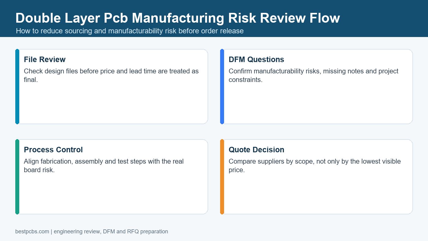
Double layer PCB manufacturing looks simple, but buyers still need to confirm vias, plated through holes, drill data, copper, solder mask, finish and test scope before production. Small file or hole-plating assumptions can affect assembly and reliability.
Use the RFQ stage to clarify board thickness, copper weight, component holes, slots, mounting holes, finish, electrical testing and assembly needs. This keeps a basic two-layer project from becoming a preventable rework issue.
What Is a Double Layer PCB?
A double layer PCB, also called a two-layer PCB or double-sided PCB, has conductive copper patterns on both sides of the board. Components can be placed on one or both sides depending on the assembly design, and vias or plated through holes connect the two copper layers.
This structure is common for projects that need more routing flexibility than a single-sided PCB but do not yet require four, six or more layers. Bestpcbs lists a dedicated single-sided and two-layer PCB service, which makes it a natural internal destination for buyers comparing basic board structures.
When a Double Layer PCB Is the Right Choice
A double layer PCB is usually the right choice when the circuit needs moderate routing density, through-hole or SMT assembly, and cost control without the complexity of a multilayer stackup. It is often used for power supplies, LED control, industrial interfaces, simple communication boards, sensor boards, control panels and consumer electronics modules.
It may not be the best choice if the design needs controlled impedance routing, dense BGAs, many power and ground planes, strict EMI control or high-speed signals that need stable return paths. In those cases, compare the design with a multilayer PCB manufacturing option before locking the board structure.
Double Layer PCB Manufacturing Process
The manufacturing process normally moves from data review to material preparation, imaging, etching, drilling, plating, solder mask, surface finish, routing, testing and packaging. The exact flow depends on the supplier, material, finish and inspection requirements, but the buyer should understand the main control points.
- Review Gerber or ODB++ files, drill data, board outline and notes.
- Prepare copper-clad laminate and apply imaging to define top and bottom circuit patterns.
- Etch unwanted copper and inspect the circuit patterns.
- Drill component holes, vias, slots or mounting holes according to the drill file.
- Plate the holes when electrical connection between both sides is required.
- Apply solder mask, silkscreen and the specified surface finish.
- Profile the board, run electrical testing and package the finished PCBs.
Stackup, Vias and Plated Through Holes
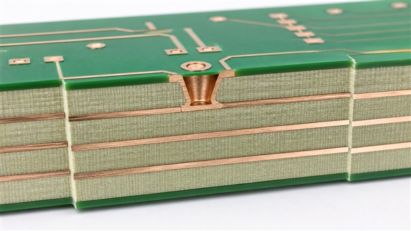
The key manufacturing feature of many double layer PCBs is the plated through hole, because it creates electrical continuity between the top and bottom copper layers. If plating, annular ring, drill tolerance or hole notes are unclear, the board can face continuity, soldering or assembly problems.
Review via size, finished hole size, drill-to-copper clearance, annular ring, component hole tolerance and slot requirements before release. If the board has connectors, large through-hole parts, high current terminals or press-fit requirements, state them clearly in the fabrication drawing.
Materials, Copper and Surface Finish Choices
Most double layer PCBs use FR-4, but the correct material, copper weight and surface finish still depend on the circuit, assembly method and operating environment. Do not treat all two-layer boards as identical just because the layer count is low.
| Decision | Common question | What to send the supplier |
|---|---|---|
| Material | Is standard FR-4 enough, or does the project need a special material? | Material target, Tg requirement if known, operating environment and assembly process. |
| Copper | Is the copper weight suitable for current and thermal needs? | Expected current load, trace width limits and heat considerations. |
| Finish | Which surface finish supports soldering, shelf life and pad geometry? | Finish preference, component pitch, assembly method and storage needs. |
If the build uses standard FR-4, the FR-4 PCB manufacturing page is a useful supporting reference. If the design has high current or heat concentration, record the actual load conditions instead of only writing “heavy copper” or “thermal design” in the notes.
DFM Checks Before Sending a Two-Layer PCB to Production
DFM review should confirm that the double layer PCB can be fabricated and assembled consistently before the order is placed. Two-layer boards are familiar to suppliers, but small mistakes in drill data, copper spacing, solder mask or panelization can still delay production.
- Check top and bottom copper polarity and layer naming.
- Confirm drill files, plated and non-plated holes, slots and board outline.
- Review annular ring, drill-to-copper clearance and via reliability.
- Check solder mask openings, silkscreen position and component polarity marks.
- Confirm copper balance, panelization, fiducials and test points if assembly is needed.
- State edge connector, gold finger, impedance, high-current or special finish needs if applicable.
For layout-side review, use a structured PCB design and manufacturing DFM guide before releasing files to the supplier.
Assembly Planning for Double Layer PCBs
Assembly planning affects the bare board design because component placement, fiducials, soldering method, panel rails and test access must be considered early. A two-layer PCB may be simple electrically but still create assembly risk if the files are incomplete.
If you need mounted components, prepare BOM, CPL, assembly drawing, polarity notes, approved substitutes and testing requirements. The PCBA service page can help buyers plan fabrication and assembly together instead of treating the bare board and component process as separate orders.
Testing and Quality Control
Quality control for double layer PCB manufacturing should verify circuit continuity, hole plating, solder mask quality, dimensions, surface finish and packaging condition. Electrical testing is especially important because the board has copper on both sides and may depend on plated connections between layers.
Ask whether the quote includes electrical test for the bare board, visual inspection, dimensional checks and any additional inspection needed for special holes, edge connectors or assembly. For production builds, also clarify sample approval, packaging, labeling and traceability expectations.
What Determines Double Layer PCB Manufacturing Cost?
Double layer PCB cost depends on material, board size, panel utilization, copper weight, drill count, surface finish, quantity, testing and assembly requirements. Two-layer boards are often cost-effective, but quote differences still come from details that may not be obvious in the keyword search.
| Cost factor | Why it changes the quote | How to reduce uncertainty |
|---|---|---|
| Board size and quantity | Affects panel use, material consumption and setup cost per board. | Send exact dimensions, quantity breaks and delivery expectations. |
| Drilling and plating | More holes and tighter tolerances add process control. | Provide clean drill files and separate plated/non-plated holes. |
| Copper and finish | Heavier copper or selected finish can change process cost. | State the real electrical and soldering requirements. |
| Assembly | BOM sourcing, SMT, through-hole and testing add labor and setup. | Send BOM, CPL, drawings and approved alternates. |
For broader pricing context, compare this with the custom PCB cost guide, then narrow the RFQ to the two-layer board requirements that actually apply to your project.
Files to Prepare for a Double Layer PCB RFQ
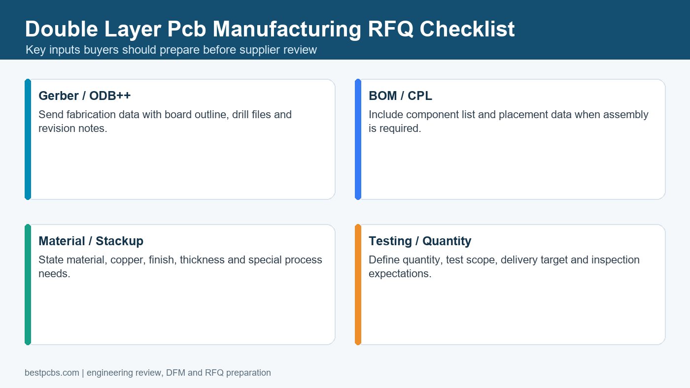
A complete RFQ package lets the supplier quote the real two-layer PCB instead of guessing from partial files. Missing drill, stackup, finish or assembly data can change both price and schedule after the first quote.
- Gerber or ODB++ files for top copper, bottom copper, solder mask, silkscreen and outline.
- Excellon drill file with plated and non-plated hole information.
- Fabrication drawing with thickness, material, copper, finish, tolerance and notes.
- Quantity, target schedule and shipment requirements.
- BOM, CPL, assembly drawing and polarity notes if PCBA is required.
- Testing, packaging, labeling and acceptance requirements.
How to Compare Double Layer PCB Suppliers
Compare suppliers by their ability to review the files, explain manufacturing assumptions and support the next production stage, not only by the lowest two-layer PCB price. A low quote is useful only when it includes the same material, finish, testing, assembly and delivery assumptions.
| Supplier question | Good answer | Warning sign |
|---|---|---|
| Can you check my drill and plated hole requirements? | They explain the review points and ask for missing files. | They quote without checking drill or fabrication notes. |
| Can you support assembly if needed? | They request BOM, CPL and assembly drawings early. | They separate fabrication and assembly without file coordination. |
| What is included in testing? | They state electrical test and any additional inspection clearly. | They use vague language such as “quality guaranteed” only. |
Common Manufacturing Risks to Avoid
The most common risks are incomplete layer data, wrong drill interpretation, unclear plated hole requirements, weak solder mask review, missing assembly files and vague testing expectations. These problems are avoidable when the RFQ package is prepared carefully.
Do not assume a two-layer PCB is too simple to need review. If the board has high current traces, tight component spacing, connector stress, unusual holes, a strict outline, or assembly on both sides, those details should be documented before the supplier starts production.
Frequently Asked Questions About Double Layer PCB Manufacturing
Is a double layer PCB the same as a two-layer PCB?
Yes. In most procurement and engineering discussions, double layer PCB, two-layer PCB and double-sided PCB refer to the same basic structure: copper circuitry on both sides of the board.
Does a double layer PCB need plated through holes?
Many double layer boards use plated through holes or vias to connect top and bottom copper layers. If the two sides do not need electrical connection, plating requirements may differ, so the drill notes should be clear.
Is a double layer PCB cheaper than a multilayer PCB?
Usually yes, because the structure is simpler. The final price still depends on size, copper, holes, finish, quantity, testing and assembly requirements.
Can Best Technology build and assemble double layer PCBs?
Bestpcbs supports PCB fabrication and PCBA services. Exact material, copper, finish, assembly and schedule requirements should be confirmed from the latest project files and process capability data before order release.
Final RFQ Recommendation
Before ordering double layer PCB manufacturing, prepare a complete RFQ package so the supplier can review the real board structure, not a guess based on the keyword or board name. Include fabrication data, drill files, material, thickness, copper, finish, quantity, testing requirements and assembly files when needed.
For a double layer PCB quote or engineering review, send your Gerber or ODB++ files, drill data, BOM, CPL, assembly drawing, quantity, material expectations, copper weight, surface finish, testing requirements and target lead time to sales@bestpcbs.com. The Best Technology / bestpcbs team can check the files, confirm what needs project-specific review, and help you prepare the board for prototype or production manufacturing.