

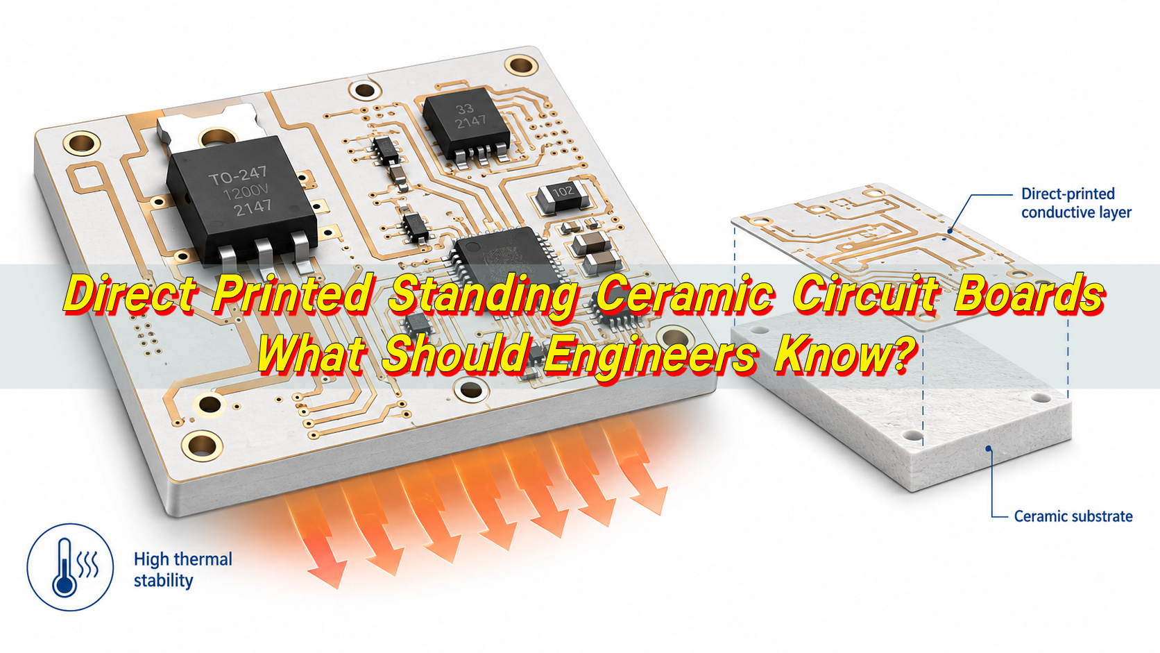
What Are Direct Printed Standing Ceramic Circuit Boards?
Direct printed standing ceramic circuit boards are ceramic-based circuit boards with conductive patterns formed directly on a ceramic substrate. They are used when a circuit must handle heat, electrical insulation, dimensional stability, and long service conditions better than a standard organic board can support.
The phrase can sound unusual because it combines several technical ideas. “Ceramic circuit boards” refers to boards made with materials such as alumina, aluminum nitride, silicon nitride, LTCC, or HTCC ceramic. “Direct printed” refers to a manufacturing method where conductive materials are applied or built directly on the ceramic surface. “Standing” may describe a board mounted vertically, used as a compact support structure, or placed in a module where space is limited.
These boards are common in power electronics, LED modules, sensors, medical equipment, industrial controls, automotive electronics, and communication systems. In these applications, the board is not only a platform for components. It also helps manage heat, maintain insulation, and support stable electrical behavior.
A direct printed ceramic board may use thick-film printing, thin-film processing, DPC, DBC, AMB, LTCC, or HTCC technology. Each process has a different conductor system, line capability, copper thickness, cost level, and application range. Engineers should select the process according to power density, operating temperature, voltage, current, assembly method, and reliability targets.
For a successful project, design review should start before prototype production. EBest Circuit usually checks key items such as line width, board thickness, conductor material, layer count, silkscreen, glass glaze, and conductive layer material before proofing. This helps reduce avoidable design changes and keeps the prototype closer to the final production requirement.
What Is a Printed Circuit Board?
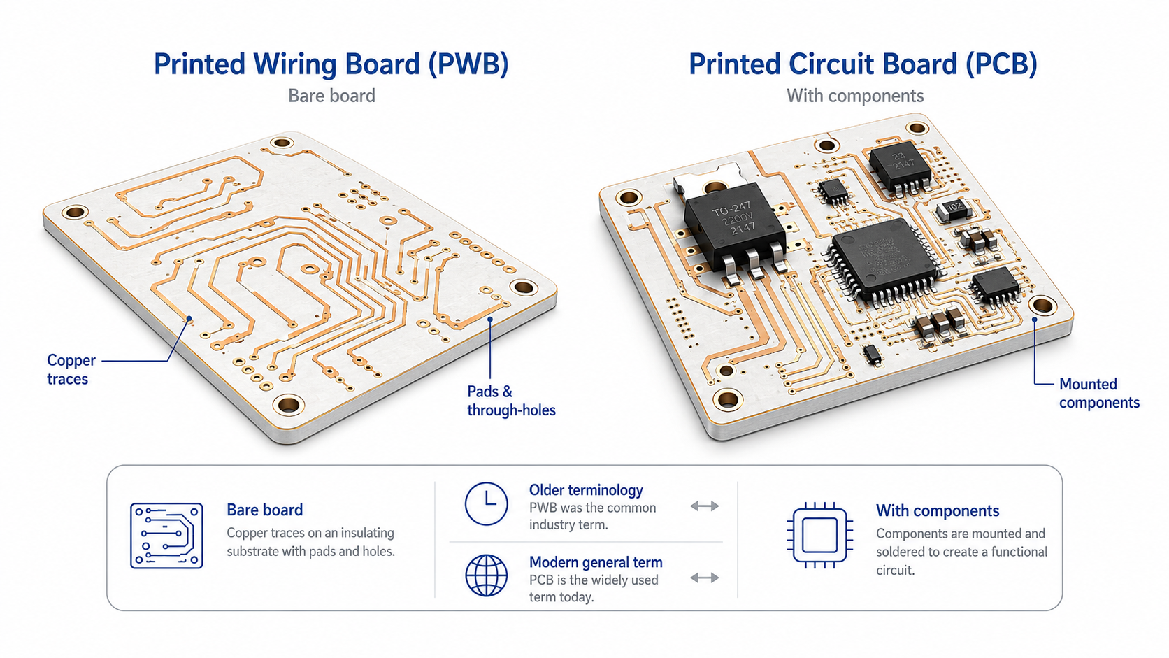
A printed circuit board, or PCB, is a board that supports and connects electronic components through designed conductive paths. These paths are usually made from copper. They replace loose wires with controlled traces, pads, vias, and layers, making electronic products smaller, cleaner, and easier to produce.
A standard PCB includes a base material, copper layers, solder mask, surface finish, vias, pads, and silkscreen. The base material provides support and insulation. Copper traces carry signals or current. Solder mask protects the copper and helps control soldering. Surface finish protects exposed pads and improves solderability. Vias connect different layers. Silkscreen provides component marks, polarity marks, logos, or assembly information.
Most rigid PCBs are made with FR4, a glass-reinforced epoxy laminate. FR4 is widely used because it offers a good balance of cost, insulation, mechanical strength, and process maturity. It works well for many control boards, communication modules, consumer electronics, industrial products, and general electronic assemblies.
A PCB may be supplied as a bare board or as a PCBA after component assembly. For ceramic projects, this distinction matters. A bare ceramic PCB is only the circuit substrate. A ceramic PCBA includes mounted components, soldering, inspection, and sometimes functional testing.
What Is the Difference Between a Printed Wiring Board and a Printed Circuit Board?
A printed wiring board, or PWB, usually refers to a bare board with conductive wiring patterns but without mounted components. A printed circuit board, or PCB, is the more common modern term and may refer to either a bare board or the general circuit board platform. In commercial electronics, PCB is used more often than PWB.
The terms are sometimes used interchangeably, but they are not always identical in technical documents. Older military, aerospace, and industrial documents may use PWB. Most current suppliers, engineers, and buyers use PCB for board fabrication and PCBA for assembled boards.
For sourcing, the safest approach is to define the deliverable clearly. If the order is for a bare ceramic substrate, state that. If the order includes components, assembly, and testing, use PCBA. If the board uses a specific ceramic process, name it directly, such as DPC ceramic PCB, DBC ceramic substrate, AMB ceramic PCB, thick-film ceramic circuit, LTCC module, or HTCC ceramic board.
| Term | Common Meaning | Component Status | Typical Use |
|---|---|---|---|
| Printed Wiring Board | Bare board with conductive wiring | Usually without components | Older technical documents |
| Printed Circuit Board | General circuit board platform | May be bare or general-use term | Modern PCB manufacturing |
| Printed Circuit Board Assembly | PCB with mounted components | With components | SMT, DIP, turnkey assembly |
| Ceramic Printed Circuit Board | PCB made on ceramic substrate | Bare or assembled | Power, LED, RF, medical, automotive, industrial |
For direct printed ceramic projects, terminology should be precise. A thick-film ceramic circuit, DPC ceramic PCB, and AMB ceramic substrate are different products. They may all be called ceramic circuit boards, but their materials, processes, and performance levels are not the same.
Why Are Ceramic Materials Used for Printed Circuit Boards?
Ceramic materials are used for printed circuit boards because they provide high thermal conductivity, strong electrical insulation, stable dimensions, and good high-temperature performance. These properties are useful when a board must support power devices, LEDs, sensors, RF modules, or compact assemblies.
Common ceramic PCB materials include alumina, aluminum nitride, and silicon nitride. Alumina is widely used because it has good insulation, mechanical strength, and cost control. Aluminum nitride is selected when higher thermal conductivity is required. Silicon nitride is often used in demanding power modules because it offers strong mechanical toughness and good thermal shock performance.
The thermal difference between FR4 and ceramic is significant. FR4 usually has thermal conductivity of about 0.3–0.4 W/m·K. Alumina ceramic is commonly around 20–30 W/m·K. Aluminum nitride can reach about 170 W/m·K or higher, depending on material grade. This helps move heat away from hot components and into a heat sink or housing.
Ceramic also provides strong dielectric performance. It can help maintain insulation in compact circuits where voltage, heat, and current are close together. This is valuable in power supplies, converters, inverters, motor drives, battery systems, high-power LEDs, medical devices, and radar communication equipment.
Engineers choose ceramic materials mainly for these reasons:
- Better heat transfer than FR4 in power-dense designs
- High electrical insulation for compact circuits
- Stable performance under high operating temperatures
- Good dimensional control during thermal cycling
- Compatibility with thick film, thin film, DPC, DBC, AMB, LTCC, and HTCC processes
Ceramic is harder and more brittle than FR4, so design and production control are important. Edge design, hole structure, metallization adhesion, copper thickness, surface finish, and assembly stress should be reviewed early.
How Are Ceramic Printed Circuit Boards Different from FR4 PCBs?
Ceramic printed circuit boards and FR4 PCBs both connect electronic components, but they are used for different performance needs. FR4 is suitable for many general electronic products. Ceramic is used when heat transfer, insulation, temperature stability, or package reliability becomes more important.
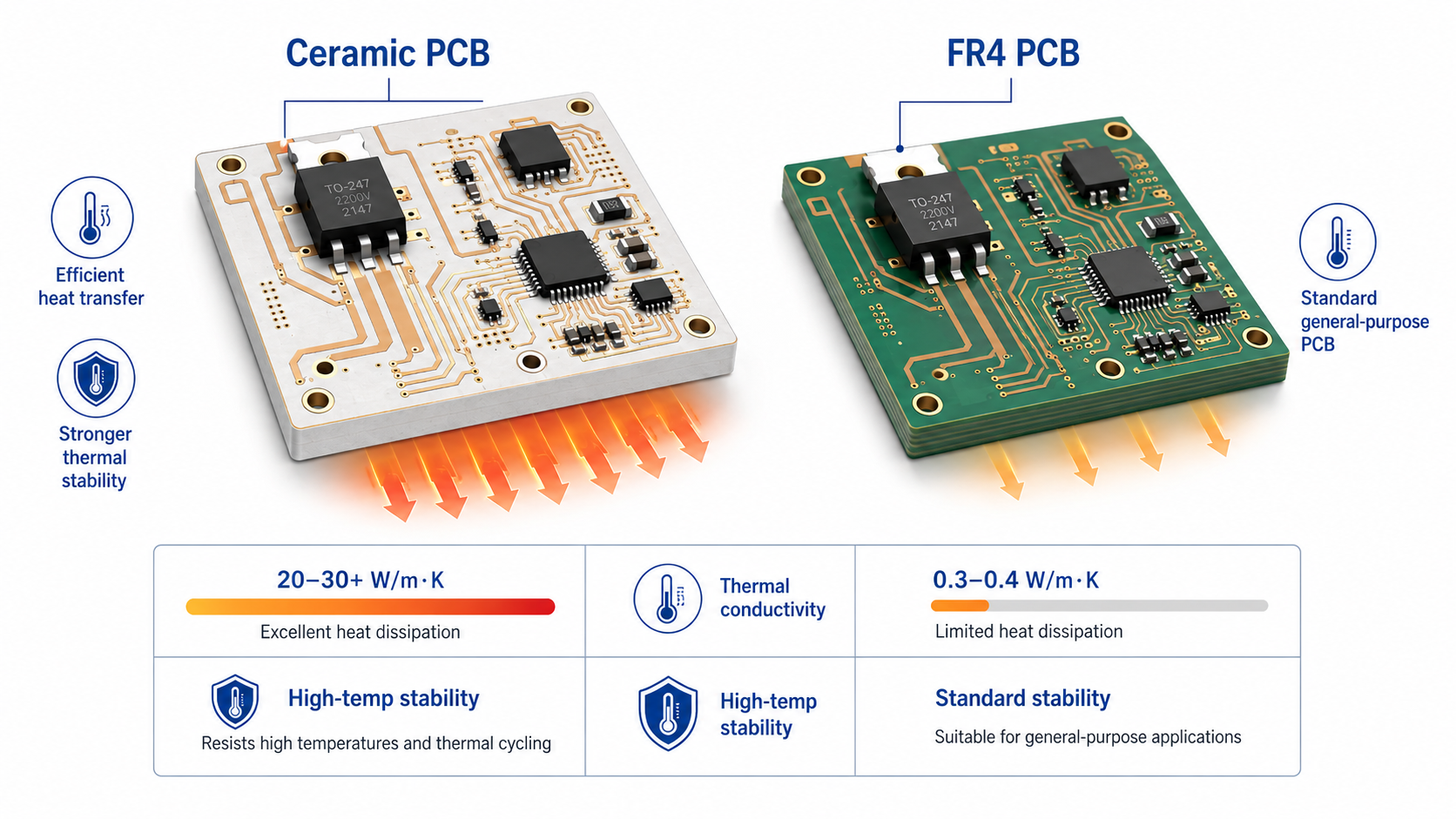
Ceramic PCBs are chosen when the board must work as part of the thermal and electrical structure. They are common in high-power LEDs, power modules, RF packages, automotive electronics, medical modules, and industrial control systems. Ceramic can move heat more efficiently and maintain stable insulation under higher stress conditions.
| Item | FR4 PCB | Ceramic Printed Circuit Board |
| Base Material | Glass-reinforced epoxy laminate | Alumina, AlN, silicon nitride, LTCC, HTCC |
| Thermal Conductivity | About 0.3–0.4 W/m·K | Alumina about 20–30 W/m·K; AlN about 170 W/m·K or higher |
| Cost Level | Lower for standard production | Higher due to material and process cost |
| Mechanical Behavior | Tough and easy to process | Hard, rigid, and dimensionally stable |
| Heat Resistance | Suitable for general electronics | Better for high-temperature applications |
| Common Applications | Consumer, industrial, communication, control boards | Power, LED, RF, medical, automotive, aerospace |
| Process Focus | Lamination, drilling, plating, etching | Metallization, firing, plating, bonding, ceramic shaping |
FR4 should remain the first choice for many standard designs because it is efficient and economical. Ceramic becomes the better choice when a standard PCB structure cannot meet thermal, voltage, or stability requirements.
What Does “Direct Printed” Mean in Circuit Board Manufacturing?
“Direct printed” means the conductive circuit pattern is formed directly on the substrate surface. In ceramic PCB manufacturing, this may involve printing conductive paste, depositing metal layers, electroplating copper, firing metallization, or using direct imaging and patterning methods.
In thick-film ceramic circuits, direct printing usually refers to screen printing conductive paste onto the ceramic substrate. The printed layer is dried and fired so the conductor bonds to the ceramic surface. Conductive materials may include silver, palladium-silver, gold, platinum-gold, or other paste systems. This process is used for hybrid circuits, sensors, heaters, resistive elements, and control modules.
In DPC ceramic PCB manufacturing, the process is different. The ceramic substrate may be laser drilled, cleaned, activated, coated with a seed layer, electroplated with copper, imaged, and etched. This allows finer circuits and thicker copper than many printed paste systems.
The phrase may also appear in discussions of digital printed circuit board technology. Digital printing can refer to inkjet conductive ink, additive electronics, or direct imaging. These methods are useful in some prototypes and special applications, but they should not be confused with high-power DPC, DBC, AMB, LTCC, or HTCC ceramic PCB processes.
How Are Direct Printed Ceramic Circuit Boards Made?
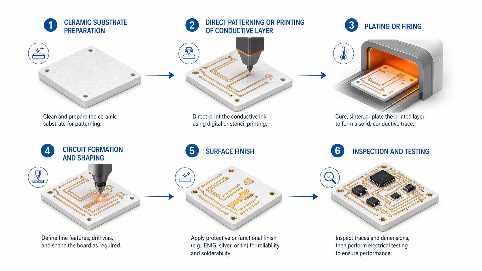
Direct printed ceramic circuit boards are made through substrate preparation, pattern formation, metallization, thermal processing, surface finishing, shaping, inspection, and testing. The process depends on the ceramic material and circuit technology.
For thick-film ceramic circuits, production starts with a cleaned ceramic substrate. Conductive paste is screen printed onto the substrate through a patterned mesh. The printed layer is dried, then fired in a controlled furnace. Additional conductive, resistive, dielectric, or protective layers can be printed and fired if the design requires them.
For DPC ceramic PCBs, the process often includes laser drilling, cleaning, seed layer deposition, copper electroplating, imaging, etching, surface finishing, and final inspection. DPC is suitable for fine circuits, high-power LEDs, laser modules, and compact thermal designs.
DBC and AMB ceramic boards use copper bonding processes instead of paste printing. DBC bonds copper directly to ceramic under high temperature. AMB uses an active metal brazing layer to bond copper to ceramic. These technologies are widely used in power modules where copper thickness, thermal transfer, and bonding strength are important.
A typical manufacturing flow includes:
- DFM review of material, conductor system, line width, spacing, copper thickness, hole structure, and surface finish
- Ceramic substrate cleaning and inspection
- Circuit pattern formation by printing, imaging, plating, bonding, or etching
- Firing, brazing, curing, or plating build-up according to the selected process
- Surface finish application for soldering, wire bonding, or die attach
- Mechanical shaping by laser cutting, scribing, CNC processing, dicing, or grinding
- Electrical test, dimensional inspection, visual inspection, and reliability checks
- Protective packaging for shipment and assembly
EBest Circuit supports thick-film, DPC, DBC, AMB, LTCC, and HTCC ceramic PCB technologies. This process range helps customers match the manufacturing method to the design instead of forcing one process into every application.
What Are the Benefits of Direct Printed Ceramic Circuit Boards?
Direct printed ceramic circuit boards offer strong thermal transfer, electrical insulation, dimensional stability, and process flexibility. These benefits make them suitable for compact and high-reliability electronic products.
Thermal performance is the main reason many engineers select ceramic. Power devices, LEDs, laser diodes, high-power resistors, and RF components can generate concentrated heat. Ceramic helps move heat away from these components more efficiently than FR4. This can support stable performance and a longer product life.
Main benefits include:
- Improved heat transfer for power and LED applications
- Strong insulation for high-voltage and compact layouts
- Stable performance under higher operating temperatures
- Good dimensional control during thermal cycling
- Compatibility with several ceramic PCB technologies
- Support for soldering, wire bonding, die attach, and hybrid assembly
The business value is also practical. A well-designed ceramic PCB can help reduce thermal risk, support compact modules, and improve product consistency. For buyers, the key is to select the correct ceramic type and process at the beginning rather than treating all ceramic PCBs as the same product.
What Applications Need Direct Printed Standing Ceramic Circuit Boards?
Direct printed standing ceramic circuit boards are used in products that need heat control, insulation, compact structure, and reliable long-term performance. They are common in power electronics, automotive electronics, medical equipment, LED systems, laser modules, industrial controls, instrumentation, RF modules, and radar communication.
Power electronics is one of the main application areas. Converters, inverters, motor drives, IGBT modules, MOSFET modules, and power supplies often require efficient heat transfer and reliable insulation. DBC and AMB ceramic substrates are often used in these products because they can support bonded copper layers and high thermal loads.
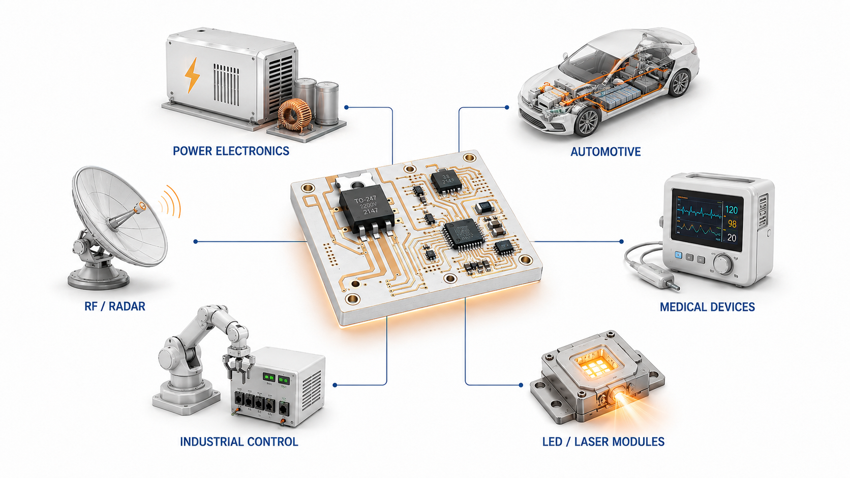
LED and laser systems also use ceramic circuit boards. High-power LEDs and laser diodes need stable heat spreading to maintain performance. DPC ceramic PCBs are common in these designs because they can support fine circuits and effective heat dissipation.
Automotive electronics often require durability under heat, vibration, and thermal cycling. Ceramic boards can be used in EV power systems, battery management, lighting modules, sensors, braking systems, and control units.
Medical equipment may use ceramic printed circuit boards in diagnostic modules, imaging equipment, surgical instruments, sensors, and precision control systems. These products often require stable performance, controlled quality, and reliable assembly.
Typical applications include:
- Power modules for converters, inverters, motor drives, and power supplies
- EV electronics, battery systems, automotive lighting, and braking control
- High-power LED, UV LED, laser diode, and optical modules
- Medical diagnostic equipment, sensors, and precision modules
- Industrial control, instrumentation, frequency conversion, and automation systems
- RF modules, radar communication, aerospace electronics, and defense-related equipment
For RFQ preparation, engineers should provide operating temperature, current, voltage, peak power, board size, ceramic type preference, surface finish, assembly method, expected lifetime, and test requirements. These details help the manufacturer recommend the correct process.
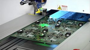
What Testing Is Needed for Ceramic Printed Circuit Boards?
Testing for ceramic printed circuit boards should verify electrical performance, dimensional accuracy, metallization quality, surface finish, thermal reliability, and assembly readiness. The test plan should match the board type and application.
Electrical testing checks opens, shorts, resistance, and insulation. For high-voltage products, dielectric withstand and insulation resistance tests may be required. These tests confirm that the board can maintain safe electrical separation during operation.
Visual and dimensional inspection checks cracks, chips, scratches, contamination, conductor defects, edge quality, hole position, board thickness, line width, spacing, pad size, and flatness. Ceramic boards are hard and rigid, so edge quality and handling control are important.
Metallization testing checks conductor adhesion, thickness, solderability, and surface finish quality. Adhesion is critical because the metal layer must remain stable during soldering, wire bonding, thermal cycling, and long-term use.
Thermal reliability testing may include thermal cycling, thermal shock, high-temperature storage, humidity exposure, power cycling, and aging. These tests are common in automotive, power electronics, outdoor LED, and industrial applications.
| Test Type | Purpose | Common Checks |
| Electrical Test | Confirms circuit connection and isolation | Opens, shorts, resistance, insulation resistance |
| Dimensional Inspection | Verifies mechanical fit | Thickness, outline, holes, pads, line width, spacing |
| Visual Inspection | Checks surface and structure | Cracks, chips, scratches, contamination, pattern defects |
| Metallization Test | Confirms conductor quality | Thickness, adhesion, solderability, plating quality |
| Surface Finish Test | Verifies assembly readiness | ENIG thickness, oxidation, solderability, bondability |
| Thermal Reliability Test | Checks performance under heat stress | Thermal cycling, thermal shock, power cycling |
| Assembly Inspection | Confirms soldering or bonding quality | AOI, X-ray, shear test, wire bond pull test |
For ceramic PCBA, additional tests may include AOI, X-ray inspection, ICT, functional testing, thermal aging, and load testing. X-ray inspection is useful for large thermal pads, power components, and solder joints where void control affects heat transfer.
Acceptance criteria should be defined before production. Useful criteria include conductor thickness, surface finish thickness, insulation resistance, solderability requirement, warpage limit, cosmetic standard, and reliability test conditions. Clear criteria help suppliers control production and help customers evaluate the delivered boards.
Direct printed standing ceramic circuit boards are suitable for designs that need efficient heat transfer, strong insulation, stable dimensions, and reliable operation in demanding environments. Engineers should confirm the ceramic material, conductor system, manufacturing process, surface finish, operating conditions, and test plan before production. For ceramic PCB design, prototype, manufacturing, or assembly support, contact EBest Circuit at sales@bestpcbs.com
You may also like


Tags: ceramic printed circuit boards, digital printed circuit board, printed wiring board vs printed circuit board