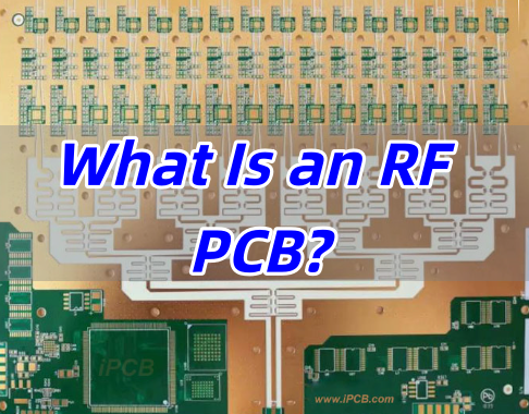
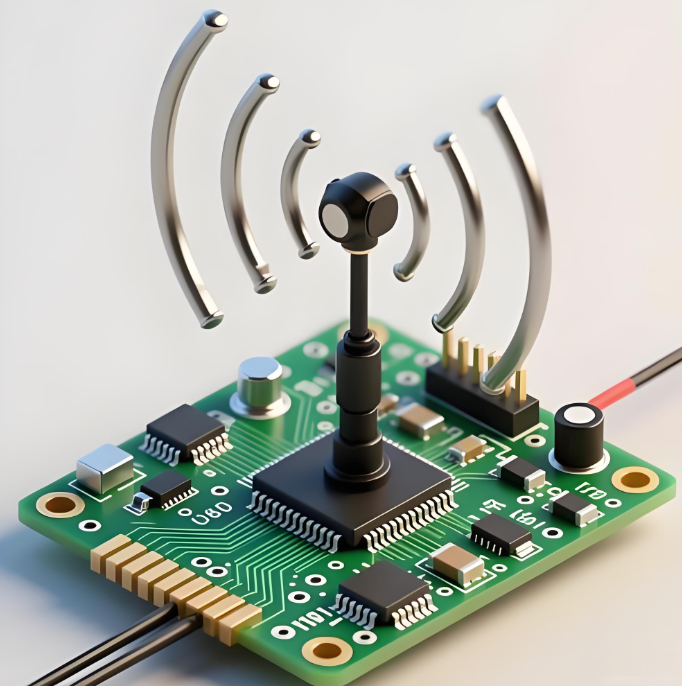
MIMO antenna is widely used in 5G CPE, LTE gateways, WiFi routers, IoT modules, UAV communication units, and industrial wireless devices. In these products, antenna performance is not only related to the antenna structure itself, but also to the PCB layout, RF trace consistency, connector reliability, controlled impedance, and PCBA assembly quality.
From a PCB and PCBA manufacturing point of view, the goal is not to redesign the antenna. The goal is to manufacture and assemble the board according to the customer’s approved RF layout, stackup, material, impedance, and assembly requirements.
Before fabrication, engineers and buyers should confirm several practical details, including RF trace width, PCB type, stackup, antenna keep-out area, controlled impedance, connector footprint, surface finish, BOM, pick-and-place file, and assembly drawing. For MIMO antenna PCB fabrication, RF PCB manufacturing, or PCBA assembly support, you can send your Gerber files, BOM, stackup, and assembly requirements to sales@bestpcbs.com for review and quotation.
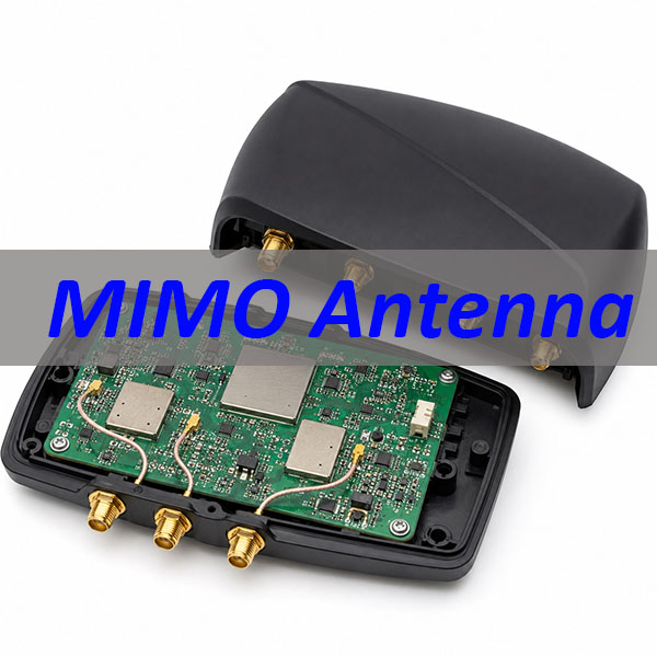
What Is a MIMO Antenna?
A MIMO antenna is an antenna system that uses multiple antenna paths to send and receive wireless signals. MIMO stands for Multiple Input, Multiple Output. It is widely used in 5G, LTE, WiFi, IoT, industrial wireless devices, routers, gateways, UAV communication units, and smart electronic products.
For engineers and buyers, the key point is not only how the antenna works in theory. In a real product, the MIMO antenna is closely connected with the PCB layout, RF feed lines, grounding area, impedance control, connectors, and PCBA assembly quality.
A typical product using a MIMO antenna may include:
- RF feed lines on the PCB
- Printed antenna areas or external antenna connectors
- Matching component pads
- Controlled impedance traces
- RF connectors such as SMA, IPEX, U.FL, or similar interfaces
- Wireless module or chipset area
- Ground reference and shielding clearance
From a PCB and PCBA manufacturing point of view, the role of the manufacturer is not to redesign the antenna. The real task is to produce the PCB and assemble the PCBA according to the customer’s approved RF layout, stackup, impedance, and assembly requirements.
For this reason, MIMO antenna projects should be reviewed carefully before fabrication. RF trace width, PCB stackup, antenna keep-out area, connector footprint, surface finish, and assembly files should all be checked early to reduce production risk.
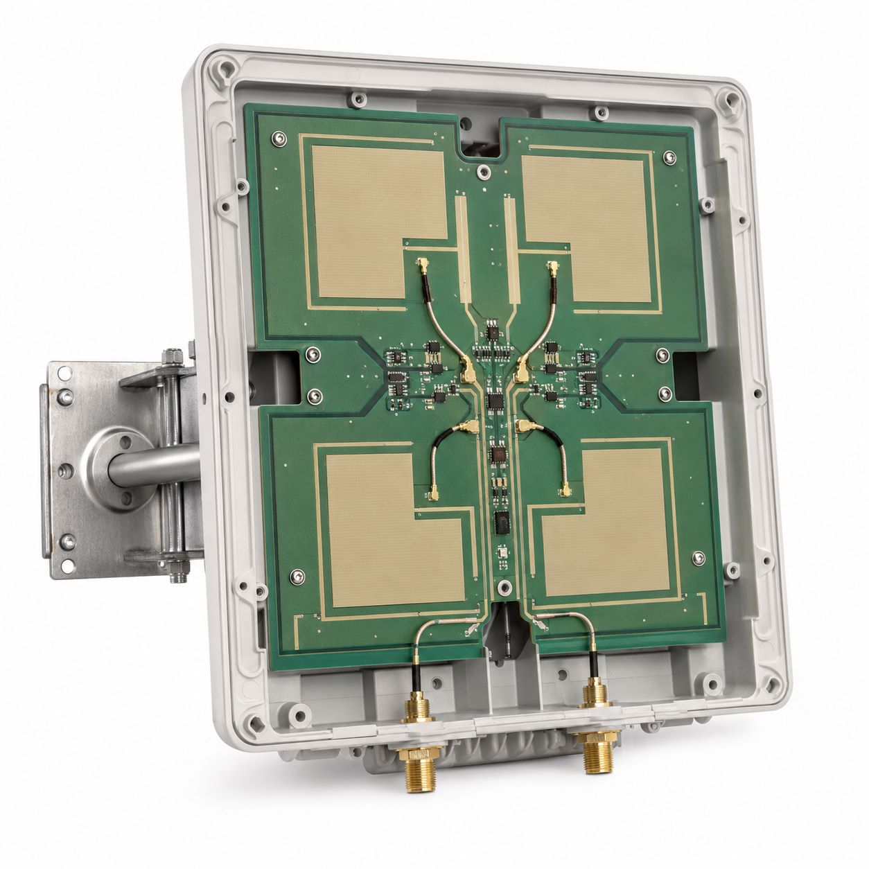
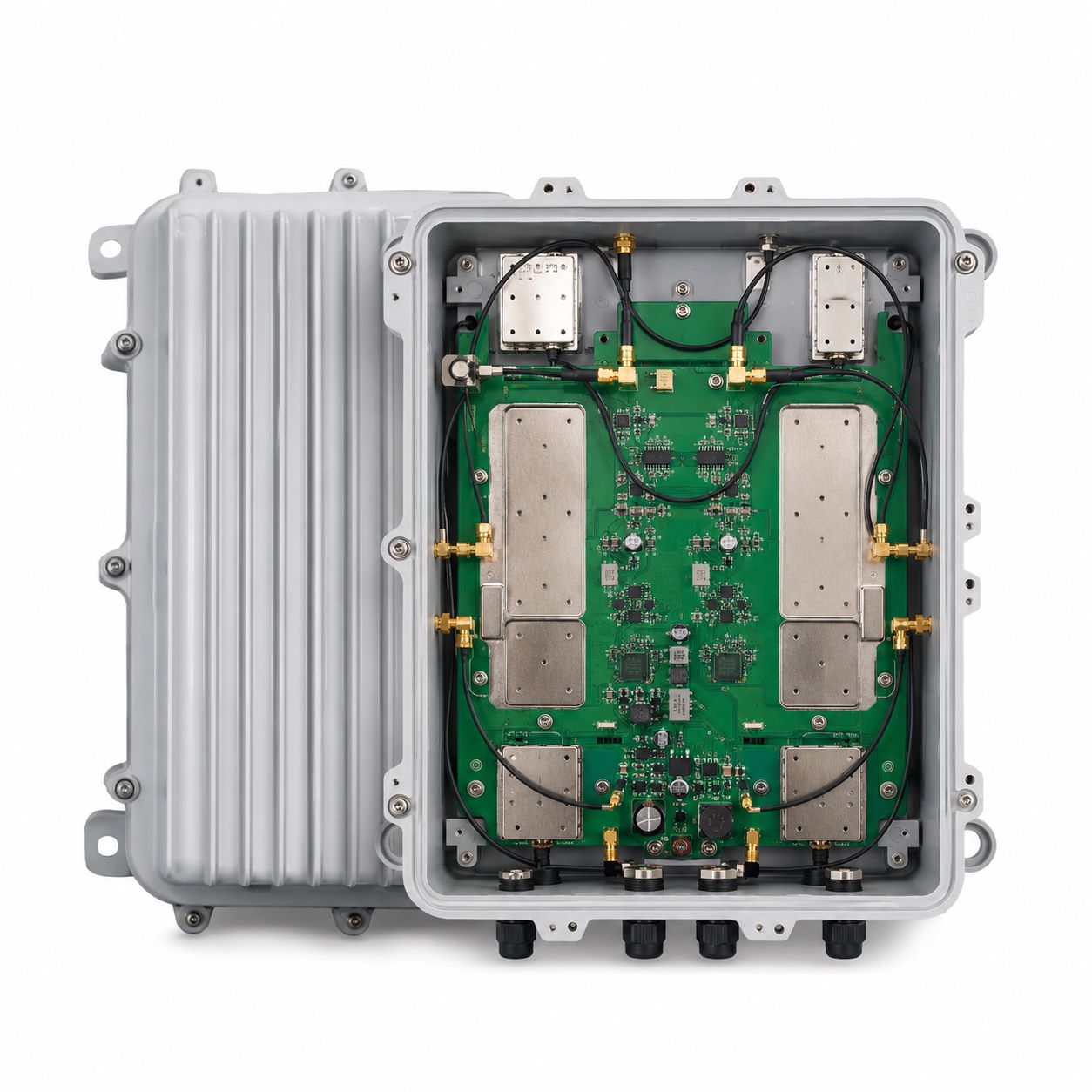
2×2 MIMO Antenna vs 4×4 MIMO Antenna PCB
A 2×2 MIMO antenna usually uses two RF paths, while a 4×4 MIMO antenna uses four RF paths. For PCB manufacturing, this difference affects layout density, connector quantity, impedance control, and PCBA inspection.
| Item | 2×2 MIMO Antenna PCB | 4×4 MIMO Antenna PCB |
|---|---|---|
| RF paths | 2 | 4 |
| Layout density | Lower | Higher |
| PCB space pressure | Lower | Higher |
| RF connectors | Fewer | More |
| Matching components | Fewer | More |
| Controlled impedance | Required | More critical |
| PCBA inspection | Moderate | More detailed |
A 4×4 board usually needs more careful RF trace routing, connector placement, antenna spacing, and assembly checking. For compact devices, layout density should be reviewed early to reduce fabrication and assembly risks.
4×4 MIMO Antenna 5G PCB Requirements
A 4×4 MIMO antenna 5G board usually has tighter PCB space and more RF paths than a basic wireless board. This makes stackup, impedance control, and connector assembly more important.
Before production, these items should be reviewed:
| Production Item | What to Confirm |
|---|---|
| PCB stackup | Dielectric thickness and layer structure |
| RF trace width | Matches the impedance calculation |
| Copper thickness | Affects etching and final impedance |
| Connector footprint | Supports soldering and mechanical strength |
| Antenna area | Keep-out area is clear |
| Surface finish | Suitable for RF connector soldering |
| PCBA files | BOM, placement file, and assembly drawing are complete |
Most RF feed lines are designed around 50Ω controlled impedance. The final trace width should be calculated based on the confirmed stackup, material data, copper thickness, and production tolerance.
LTE MIMO Antenna and 4G LTE MIMO Antenna PCB
An LTE MIMO antenna or 4G LTE MIMO antenna product often uses RF connectors, coaxial cables, module interfaces, or printed antenna areas. The PCB should support stable RF transmission and reliable assembly.
For LTE-related boards, the main manufacturing checks include:
- RF trace width and clearance
- Connector footprint accuracy
- Ground reference near RF paths
- Matching component pad size
- Board edge accuracy if the antenna is near the outline
- Surface finish for stable soldering
- PCBA inspection for connectors and small RF components
For products using external LTE antennas, connector strength and cable direction should be checked before assembly. This helps reduce mechanical stress during final product installation.
MIMO WiFi Antenna PCB for Compact Devices
A MIMO WiFi antenna board is often used in WiFi 6, WiFi 7, router, gateway, smart home, and IoT products. These products usually have compact layouts, small RF components, and limited antenna space.
For compact WiFi boards, the PCB layout review should focus on:
- Antenna keep-out area
- RF trace continuity
- Controlled impedance requirement
- Ground clearance
- Connector position
- Component height near antenna areas
- Shielding can clearance
- Assembly access for inspection
Here, PCB layout support means manufacturability review and assembly review. It does not mean changing the customer’s full RF antenna design. The approved RF structure should be protected during PCB fabrication and PCBA assembly.
External MIMO Antenna Connections for PCB/PCBA
Many wireless products use an external MIMO antenna, such as a MIMO panel antenna, directional antenna, omnidirectional antenna, FPC antenna, or coaxial antenna interface. For a PCB and PCBA manufacturer, the focus is not to select the antenna type. The focus is to make sure the antenna connection on the PCB is accurate, reliable, and easy to assemble.
The connector area should be reviewed before production because it affects soldering strength, cable direction, enclosure fit, and long-term product reliability.
| Antenna Interface | PCB/PCBA Focus |
|---|---|
| External MIMO antenna | RF connector footprint, solder pad strength, and cable direction |
| MIMO panel antenna | Connector position, enclosure clearance, and coax cable routing |
| MIMO directional antenna | Stable RF connector assembly and mechanical fixing |
| Omnidirectional MIMO antenna | Connector layout, ground area, and assembly access |
| FPC antenna | FPC connector soldering, cable bending direction, and fixture space |
| Coaxial antenna interface | U.FL, IPEX, SMA, or similar connector footprint control |
For PCBA production, RF connectors need careful inspection. Poor soldering, weak pad design, unsuitable plating, or tight cable bending may affect final assembly reliability. Before production, customers should confirm the connector type, footprint, cable direction, assembly drawing, and any mechanical clearance requirement.
PCB Types for MIMO Antenna Boards
Different wireless products may require different PCB types. The right choice depends on frequency, cost target, product size, impedance requirement, assembly structure, and reliability needs.
| PCB Type | Common Use | Manufacturing Focus |
|---|---|---|
| FR4 PCB | Basic WiFi, IoT, and cost-sensitive wireless boards | Mature process and cost-effective production |
| High-Tg PCB | Industrial wireless modules and long-running devices | Better thermal stability |
| RF PCB | 5G, LTE, WiFi, and RF modules | Impedance, dielectric thickness, and RF trace control |
| Rogers PCB | High-frequency and low-loss wireless products | Stable dielectric performance for higher-frequency applications |
| Hybrid Stackup PCB | RF + digital mixed circuits | Balances RF performance, cost, and structure |
| Rigid-Flex PCB | Space-limited wireless devices | Supports compact structure and reliable interconnection |
For MIMO antenna PCB projects, PCB type selection should not be based only on price. It should match the RF path, stackup, impedance requirement, connector type, and PCBA assembly method.
Before production, these details should be confirmed:
- PCB type
- Material grade
- Board thickness
- Copper thickness
- Stackup structure
- Impedance requirement
- Surface finish
- Assembly method
- Material availability
For RF-related projects, PCB type or material replacement should be handled carefully. Even when two options look similar, changes in dielectric constant, board thickness, copper type, or stackup may affect impedance result and production consistency.
MIMO Antenna PCB Layout and DFM Review
For this topic, PCB layout means layout support for manufacturability and assembly. It does not mean full antenna design or RF system redesign.
A practical DFM review should check whether the approved RF layout can be fabricated and assembled reliably.
| Layout Area | DFM Review Point |
|---|---|
| Antenna keep-out area | No unexpected copper, screws, cables, or tall components |
| RF feed line | Short, clean, and impedance-controlled |
| Ground area | Stable ground reference and proper clearance |
| Matching component pads | Accurate pad size and easy assembly |
| Connector placement | Suitable for cable direction and inspection |
| Shielding area | Enough clearance from RF-sensitive areas |
| Board outline | Correct mechanical fit and antenna edge control |
For faster review, customers should provide Gerber files, PCB stackup, impedance requirement, BOM, pick-and-place file, assembly drawing, and RF notes.
MIMO Antenna PCB Manufacturing and PCBA Inspection
For MIMO antenna PCB manufacturing, the most important point is repeatability. A PCB supplier should help keep the same stackup, copper geometry, impedance result, and assembly quality from prototype to batch production.
Key manufacturing controls include:
| Control Item | What to Check |
|---|---|
| Stackup control | Dielectric thickness and layer structure |
| Controlled impedance | RF trace width, copper thickness, and tolerance |
| Etching accuracy | RF trace shape and spacing |
| Board outline | Antenna edge and mechanical fit |
| Surface finish | Solderability and connector reliability |
| Solder mask | Clearance around RF-sensitive areas |
| AOI inspection | Trace shape and copper defects |
| Electrical test | Continuity and isolation |
| PCBA inspection | RF connector and matching component quality |
For PCBA assembly, special attention should be given to:
- RF connector soldering
- Small matching components
- Shielding can position
- Coax cable direction
- Connector mechanical strength
- Cleanliness around RF areas
- X-ray inspection when required
EBest Circuit supports PCB fabrication, RF board material selection, controlled impedance, DFM review, component sourcing, PCBA assembly, AOI, X-ray, electrical testing, and production follow-up for wireless electronic products.
FAQs About MIMO Antenna
Q1: What is a MIMO antenna?
A MIMO antenna uses multiple antenna paths to improve wireless speed, coverage, and connection stability.
Q2: What is a MIMO antenna PCB?
It is a PCB that carries antenna areas, RF feed lines, matching components, connectors, grounding areas, and related wireless circuits.
Q3: What is the difference between 2×2 and 4×4 MIMO antenna PCB?
A 2×2 board has two RF paths, while a 4×4 board has four. A 4×4 board usually needs more PCB space, better routing control, and more careful PCBA inspection.
Q4: What should be checked for a 4×4 MIMO antenna 5G PCB?
The stackup, RF trace width, impedance requirement, antenna keep-out area, connector footprint, surface finish, and assembly files should be checked before production.
Q5: Can FR4 be used for MIMO WiFi antenna PCB?
Yes. FR4 can be used for some WiFi and IoT products. For higher-frequency or lower-loss applications, RF PCB, Rogers PCB, or hybrid stackup PCB may be considered.
Q6: Does MIMO antenna PCB need controlled impedance?
Yes. RF feed lines usually require controlled impedance, commonly 50Ω, to support stable RF transmission.
Q7: What PCB type is used for MIMO antenna boards?
Common options include FR4 PCB, High-Tg PCB, RF PCB, Rogers PCB, Hybrid Stackup PCB, and Rigid-Flex PCB. The choice depends on frequency, stackup, impedance, cost, and assembly structure.
Q8: What should be checked for external MIMO antenna connections?
RF connector footprint, solder strength, cable direction, mechanical clearance, plating quality, and PCBA inspection should be checked.
Q9: Can EBest Circuit manufacture MIMO antenna PCB and PCBA?
Yes. EBest Circuit can support MIMO antenna PCB fabrication, controlled impedance, RF material selection, DFM review, component sourcing, PCBA assembly, and testing. Send your Gerber, stackup, BOM, and assembly files to sales@bestpcbs.com for a quotation.