

Gold fingers are one of the most critical features in many circuit boards, especially those used in high-reliability connections. Whether you’re building a test interface, designing a PCIe card, or creating an edge connector, understanding gold finger beveling and its plating design is essential for durability and smooth performance.
Let’s explore everything about PCB gold fingers, the beveling process, and how to choose the right beveling angle for your board design.
What Is a Gold Finger?
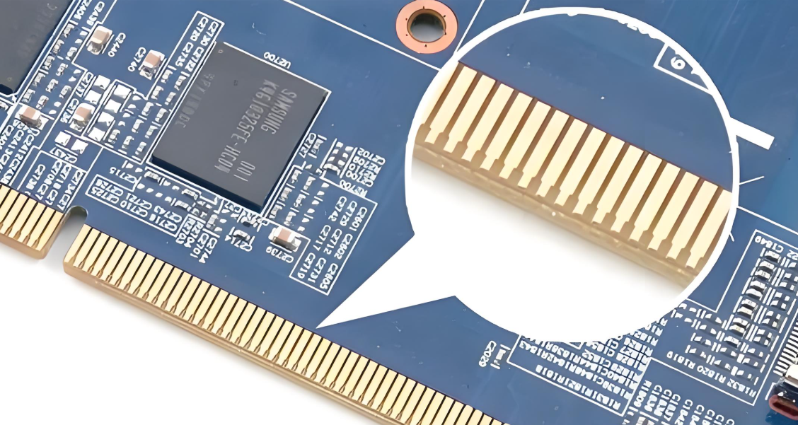
PCB gold fingers are the gold-plated connectors located along the edge of a printed circuit board. They serve as contact points when a PCB is inserted into a slot or connector, just like in RAM, GPU cards, or other modular systems. These fingers are plated with hard gold to ensure they can withstand repeated insertion and removal cycles without wearing out.
They are called “fingers” because they look like narrow, elongated pads stretching along the PCB’s edge, similar to the fingers of a hand. Each gold finger connects to a circuit trace inside the board. When the PCB is inserted into a slot, the metal contacts on the gold fingers align with the contacts inside the connector, allowing signals to pass through.
The main reason gold is used is because it doesn’t corrode easily. Gold provides high conductivity and can withstand many insertions without losing its shape or functionality. In critical environments—like military, aerospace, or telecom—this reliability is essential.
Types of Gold Fingers in PCB
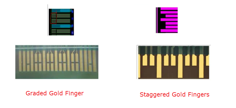
PCB gold fingers can be divided into two types – graded gold fingers and staggered gold fingers.
- Graded Gold Finger
Graded gold fingers refer to a design where the fingers are plated with gold at varying lengths or staggered elevations. Instead of all the fingers being aligned in a straight line, some are slightly longer than others. This is not just a visual variation—it serves a very specific purpose. Graded fingers are typically used in applications where controlled insertion sequencing is required. When the PCB is inserted into the slot, the longer fingers make contact first, followed by the shorter ones.
- Staggered Gold Fingers
Another design strategy is using long and short gold fingers—also known as staggered gold fingers. This refers to gold fingers of different physical lengths on the same board edge, but typically without beveling or plating depth variation. This technique is commonly used in:
- PCIe hot-pluggable cards
- Industrial control systems with replaceable modules
- Burn-in or test fixtures requiring safe first-contact
The lengths are designed based on the depth of the connector slot and how the PCB enters the socket. Sometimes only a few pins—such as GND or VCC—are made longer, while the rest remain short.
How Thick Is PCB Gold Finger Plating?
The durability of gold fingers comes from their plating thickness. Not all gold fingers are created equal. The thickness of the plating affects both how well they perform and how long they last.
The gold layer is not pure; it is electroplated hard gold, which includes a bit of cobalt to improve hardness and wear resistance. Here’s a breakdown of common thicknesses:
| Application Type | Gold Plating Thickness (Hard Gold) |
| Standard Consumer Devices | 0.76μm (30μin) |
| Industrial or Light Insertion | 1.27μm (50μin) |
| High-Durability Applications | 2.54μm (100μin) |
In general, 50μin is the most common for boards that are plugged and unplugged many times. If the fingers are not meant to be removed often, thinner plating is usually fine. But when in doubt, thicker is better—it provides stronger wear resistance.
What Is the Process of Gold Plating in PCB?
Creating strong, reliable pcb gold fingers requires precision. The plating process is done after the rest of the board is fabricated and cleaned. The focus is to add a hard gold layer only to the fingers—nowhere else. Here’s how the PCB gold finger plating process works step-by-step:
1. Finger Area Isolation
First, the PCB is cleaned, and only the finger areas are exposed. The rest of the board is masked to prevent unwanted plating elsewhere.
2. Nickel Plating (Bottom layer)
A nickel layer (typically 3–6μm) is electroplated onto the copper finger base. Nickel improves gold adhesion and acts as a barrier to prevent copper from diffusing into the gold over time.
3. Gold Electroplating (Top Layer)
After nickel, a layer of hard gold is plated on top. This layer is usually between 30μin and 100μin depending on the application. The plating uses a current that drives gold ions onto the nickel surface.
4. Cleaning and Inspection
Once the plating is complete, the board is cleaned, and the gold fingers are inspected for uniformity, roughness, or any missing areas.
5. Beveling (If Required)
If beveling is needed, it is done after plating. The edge is shaped to allow easier insertion into connectors.
6. Final Finishing
The rest of the PCB receives its finish (e.g., ENIG, OSP, HASL), but gold fingers remain untouched.
This plating method results in durable, smooth connectors that resist oxidation and mechanical wear.
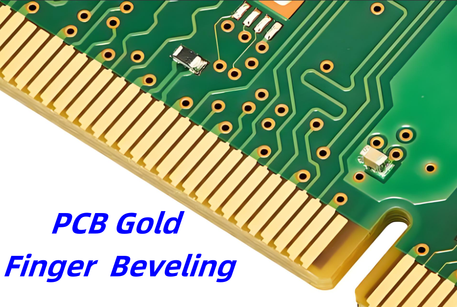
What Is Gold Finger Beveling?
Gold finger beveling is a mechanical process that trims the edge of the PCB—where the gold fingers are located—into a sloped angle. Rather than a blunt 90° edge, the bevel creates a smooth ramp-like surface.
Imagine sliding a PCB into a connector. A sharp edge might catch, damage the connector, or scrape off the plating. But a beveled edge slides in smoothly, reducing friction and improving contact.
This is especially useful for PCBs used in:
- Backplane systems
- Server racks
- Communication modules
- Plug-and-play components
The beveling process is typically done using precision grinding or CNC milling. Care is taken to maintain exact angle measurements without overcutting the gold plating.
Purpose of Gold Finger Beveling
There are several important reasons why beveling is applied to PCB gold fingers:
- Easier Insertion
A beveled edge helps the PCB slide into the connector smoothly. It reduces the chance of misalignment or jamming.
- Prevents Contact Damage
Without beveling, the sharp PCB edge can scratch the connector pins, causing early wear or performance issues.
- Reduces Wear and Tear
Repeated insertion cycles can wear out the gold plating. Beveling distributes the pressure more evenly, extending the lifespan of both board and connector.
- Better Electrical Contact
Smoother insertion means better alignment and tighter contact with the metal pins inside the slot. This leads to more stable signals and fewer connection errors.
- Professional Manufacturing Finish
Beveled gold fingers look more refined, signaling high-quality PCB craftsmanship.
For any board that’s going to be removed and reinserted frequently, beveling is not just a good idea—it’s almost essential.
Gold Finger Beveling Angle Options
When beveling, you have options for the bevel angle. The choice depends on how the PCB fits into its slot and the degree of insertion force you want to reduce. Here are the common beveling angles:
| Angle | Description |
| 30° | The most popular angle. Balances mechanical strength and ease of insertion. |
| 40° | Offers a smoother slope than 30°. Used when insertion needs to be gentle. |
| 45° | The steepest slope. Useful when the board must glide into the slot with minimal resistance. |
Most applications stick with 30°, but you should always check the connector specification. Some high-density or high-speed connectors might require tighter tolerances and smoother entry paths.
Considerations of Beveling Angles
Before you finalize your beveling angle, consider the following:
- Slot Geometry
Look at how your connector or socket is shaped. If the slot opening is narrow, a steeper bevel (like 45°) might be helpful.
- Insertion Frequency
If the PCB will be removed often—like in test or modular setups—a smoother entry reduces long-term damage.
- Mechanical Strength
Sharper bevels remove more material. If your board edge carries mechanical load, avoid overly steep bevels.
- Gold Coverage
The beveling process should never cut through the gold. Make sure the gold plating thickness is enough to cover the entire bevel.
- IPC Guidelines
Refer to IPC-6012 and IPC-A-600 for guidelines on gold finger design, plating, and beveling requirements.
Always coordinate with your PCB manufacturer to ensure the chosen bevel angle is feasible and matches your product’s functional needs.
PCB Gold Fingers Applications
Gold fingers are everywhere. Any device that uses edge connectors likely has them. Some of the most common use cases include:
- Graphics cards (GPU) – for connecting with the motherboard
- RAM modules – inserted into DIMM slots
- Motherboards and backplanes – for communication between layers or devices
- Test interface boards – for burn-in, programming, or debugging
- PLC and industrial control systems – for module plug-in
- Medical and defense electronics – where reliability is critical
In all these applications, gold finger beveling helps ensure the boards don’t fail during connection or removal. It may seem like a small detail, but its effect on reliability is huge. Gold finger beveling is one of those small but powerful features that improves the mechanical fit, electrical contact, and overall durability of your circuit boards. When designing your next PCB, pay attention to:
- The gold finger plating thickness
- Whether beveling is needed
- The best angle for smooth insertion
- And the wear-and-tear the board will experience
These decisions affect not only how well the board works, but how long it lasts.
About EBest Circuit (Best Technology)
At EBest Circuit (Best Technology), we specialize in PCB manufacturing with a focus on high-reliability boards. We handle everything from custom hard gold finger design to precision beveling, ensuring your edge connectors meet international standards. Our team works with industries including medical, automotive, aerospace, and telecom.
We follow strict quality processes and use MES traceability systems to track every step. Whether you need quick prototypes or high-volume production, our engineers are ready to help you design, test, and deliver high-performance PCBs with durable gold fingers.
Looking for a PCB manufacturer that understands the details? Let’s build your next project together.
FAQs
1. Can I design gold fingers without beveling?
Yes, but for any board that will be plugged in and out regularly, beveling is highly recommended for smoother insertion and longer lifespan.
2. What’s the difference between ENIG and hard gold?
ENIG is used on pads for soldering. Hard gold is plated on fingers for wear resistance. They are different in composition and use.
3. How do I specify beveling on my Gerber files?
You should include a separate mechanical drawing or notation in the fabrication notes to indicate the beveling angle and location.
4. Are gold fingers more expensive to produce?
Yes, due to the electroplating process and gold material cost. However, they add significant durability and value.
5. Can gold finger plating wear off?
Over time, yes—especially if the plating is thin. Using thicker plating like 50μin or more helps prevent this.
You may also like


Tags: gold finger beveling