PCB drill wander is unintended lateral movement of a mechanical drill as it enters and travels through a production panel. The finished hole can deviate from its programmed path, reducing annular ring, moving closer to internal copper or creating a non-straight hole wall.
An off-center hole is not automatically proof of drill wander. Image-to-drill registration, layer shift, artwork scaling and lamination movement can create a similar top-view result. A useful investigation separates the drill path from the copper-layer positions before selecting corrective action.
What PCB Drill Wander Means
A wandering drill does not follow the intended axis consistently through the panel stack. Deflection may begin at entry, grow with depth or change as the tool crosses different materials. The entry and exit locations can therefore tell only part of the story.
The risk rises when the hole is small relative to drilling depth, the stack is unstable, the tool is worn or running inaccurately, or feed/speed and chip removal are not suited to the construction.
Drill Wander vs Layer-to-Drill Registration Error
Drill wander describes the physical hole path; registration error describes the relationship between that path and copper features. A straight hole can look off-center if an inner layer shifted. A wandering hole can enter near center but approach an internal land at depth.
| Observation | Possible mechanism | Evidence to review |
| Entry and exit displaced similarly | Machine/program/panel registration | Tool coordinates, targets and first-piece measurement |
| Hole path bends through depth | Tool deflection or wander | Cross-section and entry/exit comparison |
| Different inner layers show different land offset | Layer registration or lamination movement | Layer targets and coupon cross-section |
| Problem increases as a bit is used | Wear, debris or runout | Tool-life and spindle records |
Why a PCB Drill Bit Deflects
The tool follows the combined mechanical forces at entry and throughout the cut. If those forces are uneven, a slender drill can bend away from the programmed axis.
- Surface texture or unsuitable entry material can disturb initial centering.
- Excess panel-stack height increases the unsupported cutting path.
- Worn or damaged cutting edges create unequal load.
- Spindle runout and poor collet condition move the tool off axis.
- Incorrect feed, speed or retraction can increase heat and deflection.
- Poor debris removal can recut chips and load the flutes.
- Construction changes can alter cutting resistance through the stack.
Entry Material, Panel Stack, and Backer Control
The drill must enter cleanly, hold its path through every panel and exit without excessive burr or breakout. Entry and backing materials support those tasks, while stack height affects rigidity, heat and chip evacuation.
A production route should match the tool diameter and board construction. Increasing the number of panels per drill stack may improve throughput, but it also changes the path length and process margin. The qualified setup—not a universal stack count—should determine the limit.
Seeing reduced annular ring or unexplained hole offset?
Send the stackup, drill files, finished-hole requirements, copper images and inspection evidence. EBest Circuit can help separate design clearance from drilling and registration risk.
Tool Wear, Runout, and Drilling Parameters
Drill-condition controls should be tied to measured output. Tool-life limits, spindle maintenance, collet cleanliness and first-piece verification help keep a process stable, but the correct thresholds depend on the tool and construction.
Feed that is too aggressive can increase lateral force; an unsuitable speed can raise heat or wear. Slow is not automatically safe: rubbing rather than cutting can also damage the hole. Process engineers qualify the combination and monitor changes rather than adjusting one parameter in isolation.
How Laminate Construction and Hole Geometry Change the Risk
A hole must be evaluated against total drilling depth, material system, copper distribution and nearby features. Thick builds and small tools deserve additional review because stiffness and chip evacuation become more demanding.
Hole type also matters. Through holes, press-fit holes, component leads, vias and controlled-depth features have different finished-size and structural priorities. For size selection, see the standard PCB drill-size guide. Controlled-depth work is covered in our controlled-depth drilling guide.
Annular Ring and Hole-to-Copper Clearance Risks
Drill movement consumes the registration allowance built into pads and clearances. The critical question is the finished relationship at every connected and nonconnected layer—not whether the drill symbol was centered in CAD.
Possible results include reduced annular ring, tangency, breakout, unwanted approach to plane copper, or a weakened connection. Pad size should be reviewed with finished-hole tolerance, plating allowance and the fabricator’s registration capability. See the PCB annular ring guide for the geometry.
Hole-Wall and Plating Consequences
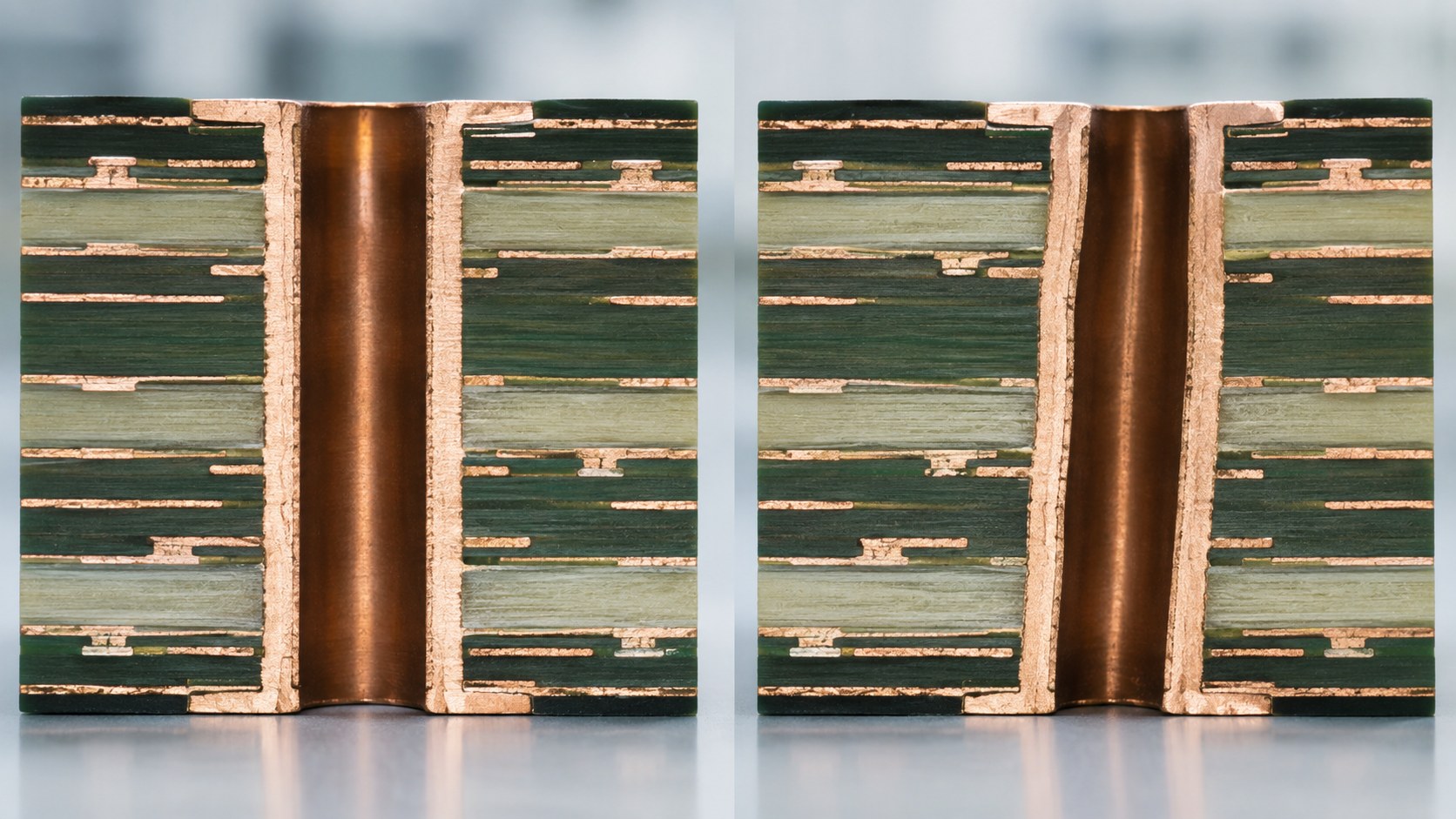
A non-straight or rough drilled hole can complicate desmear, activation and copper deposition. Drill smear, debris, wall roughness or local geometry changes may affect how the plated barrel forms.
Do not assume every offset hole has a plating defect, and do not assume good continuity proves the complete wall is acceptable. Review hole-wall condition, copper coverage and connection geometry using the agreed acceptance plan.
How PCB Drill Wander Is Detected
Detection works best when top-view measurement is combined with depth-sensitive evidence. Automated optical inspection or coordinate measurement can find entry-position trends. Exit-side review can reveal accumulated deviation. Cross-sections show the path relative to inner lands and wall condition.
Coupon and panel mapping are important when a defect changes with machine position, stack location or tool life. Record the drill program, tool identity, hit count, panel stack and measurement location so the pattern can be reproduced.
DFM Actions Before PCB Release
- Define finished rather than only nominal drill sizes.
- Provide a clear plated/non-plated and tolerance table.
- Check pad and plane clearances at every layer.
- Flag press-fit, connector and other function-critical holes.
- Review small holes against the actual construction depth.
- Avoid ambiguous duplicate drill entries or mixed units.
- Confirm how controlled-depth or backdrilled features are identified.
- Request approval before any geometry change that affects function.
What to Ask After a Drill-Position Nonconformance
A corrective-action response should identify the mechanism, affected scope and evidence of containment. Ask whether the path wandered, copper layers shifted, the panel registered incorrectly, or several factors combined.
Useful evidence includes mapped measurements, cross-sections, tool-life data, spindle/collet checks, stack setup, entry/backer lot and first-piece records. The supplier should explain how affected inventory was identified and how the revised control will be verified.
Need evidence before accepting a drilled-hole deviation?
Share the drawing, photos, measurement report, cross-sections and lot history. We can help frame the containment and acceptance questions.
What to Send for EBest Circuit Drilling Review and Quotation
Send Gerber or ODB++, NC drill files, stackup, material and copper requirements, finished-hole table, tolerances, quantities, assembly requirements, test needs and target delivery. Identify press-fit and other critical holes and provide connector specifications when relevant.
EBest Circuit can review file consistency, pad/clearance relationships and drilling-risk questions before quotation. Specific drill, aspect-ratio or tolerance capability must be confirmed against the current construction and approved production route.
PCB Drill Wander FAQ
What is PCB drill wander?
It is unintended lateral deflection of a mechanical drill from its programmed axis as it enters or travels through a PCB production stack.
Is every off-center hole caused by drill wander?
No. Artwork, layer and drill registration errors can create a similar top-view appearance.
How does drill wander affect annular ring?
It moves the finished hole toward a pad edge, reducing the remaining copper land and potentially causing tangency or breakout.
Can a worn drill cause wandering?
Yes. Uneven wear or damage can increase lateral cutting forces, although the complete machine and setup should be investigated.
Does a taller panel stack increase risk?
It increases the drilling path and can reduce margin for small tools; the qualified stack limit depends on construction and process.
Can AOI detect drill wander?
Top-view inspection can reveal hole-to-pad offset trends, but cross-section or entry/exit evidence may be needed to prove path deflection.
Can electrical test find every drill-wander problem?
No. It can identify open/short conditions but may not fully characterize remaining land, hole-wall geometry or latent structural risk.
Should designers increase every via pad?
No. Pad changes consume routing space and should be based on the actual tolerance budget and functional requirements.
What records help identify the root cause?
Tool identity and hit count, spindle/collet checks, drill parameters, stack setup, panel mapping, targets and cross-sections are useful.
What files are needed for drilling DFM?
Provide artwork, NC drill data, stackup, hole table, tolerances, critical-hole notes, quantities and any applicable component specifications.
Protect annular ring and plated-hole reliability before production.
Send your board data, hole table, stackup, quantities and target delivery for a project-specific review.