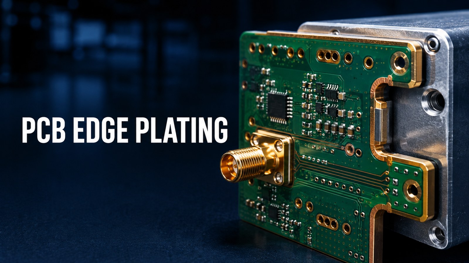
PCB edge plating is copper and final finish carried from the top or bottom conductor around a routed board edge. It is used for purposes such as RF shielding continuity, chassis grounding, mechanical contact or a plated boundary. The feature succeeds only when the copper artwork, board profile, solder-mask opening, net assignment and production panel all describe the same intent.
The safest design approach is to treat the plated edge as a manufactured three-dimensional feature—not as a decorative line on one Gerber layer. Define which edges are plated, which net owns them, where plating must stop and how the fabricator may support the board during processing. This PCB edge plating design guide turns those decisions into a DFM- and RFQ-ready package.
What Is PCB Edge Plating and When Is It Worth Using?
Edge plating wraps conductive metal over a selected external board edge so it connects intended copper features on the board faces. Depending on the design, it can close part of an RF shield boundary, provide a low-inductance connection to an enclosure, create a durable contact surface or join top and bottom ground regions along the perimeter.
It is worth specifying when the electrical or mechanical function genuinely requires a plated routed edge. It is not automatically better than perimeter vias, a metal frame, a connector shell or castellated holes. Each alternative creates a different current path, assembly interface and manufacturing constraint.
- Good candidates: RF modules fitted into conductive housings, shielding partitions, grounding rails and board edges intended to contact a conductive chassis.
- Questionable candidates: cosmetic gold edges, edges broken by many panel tabs, mixed-net copper near the route or designs without a defined mating interface.
- Required decision: state the electrical purpose and the mating condition before drawing the feature.
Edge Plating vs Castellated Holes and Edge Contacts
These features can all expose metal at a PCB edge, but they solve different problems. Selecting the wrong one can create unnecessary cost or an interface that cannot be assembled reliably.
| Feature | Main purpose | Key data to define |
| Continuous or selective edge plating | Conductive wrap, shielding boundary, chassis or mechanical contact | Plated segments, net, profile, panel breaks and finish |
| Castellated holes | Solderable half-holes for mounting one PCB onto another | Hole size, pitch, pad geometry, finished profile and assembly fillet |
| Edge-card contacts | Mating fingers for a connector | Contact pattern, bevel, finish, mask opening and connector tolerance |
| Via fence near an edge | Ground stitching and field containment without a plated route | Via pitch, return-path geometry and distance to profile |
A design may combine a via fence with edge plating, but their roles should remain explicit. If the real requirement is a solderable board-to-board interface, use a controlled castellated-hole design rather than asking a fabricator to infer it from a plated outline.
How Edge Plating Supports RF Grounding and EMC
A grounded plated edge can reduce discontinuity around a board perimeter and provide a short connection between face copper and a conductive enclosure. This is useful where RF currents need a controlled return path or where an enclosure seam should not become an unintended slot antenna.
Edge plating is not a universal EMI cure. Its effect depends on the full current path: reference planes, stitching vias, enclosure contact pressure, apertures, connector bonding and the location of high-frequency sources all matter. A continuous-looking copper edge that is poorly connected to the intended reference can add metal without fixing the actual return-path problem.
Start with the electromagnetic function, then model or review the transition. The site’s RF PCB capability overview provides context for high-frequency board construction, while this guide focuses on the plated boundary itself.
Should the Plated Edge Connect to System Ground or Chassis Ground?
Assign the plated edge to the net required by the product grounding architecture; do not default to a generic ground symbol. Signal ground, protective earth and chassis can be joined directly, joined through a defined network or kept separate depending on safety, EMC and system requirements.
- Show the plated edge on the schematic or controlled mechanical/electrical drawing with a named net.
- Identify where the edge contacts the housing and whether contact is continuous or limited to selected zones.
- Keep unrelated power or signal copper away from the plated route according to the approved DFM clearance.
- Review connector shields and mounting hardware as parts of the same grounding path.
- If chassis and circuit ground are intentionally separated, mark the isolation boundary clearly.
For high-frequency designs, the via pattern that connects surface copper to internal reference planes may be as important as the plated edge. Ask for a stackup-aware review instead of applying a copied spacing rule from another board.
How to Draw Edge Copper in the PCB Layout
Draw copper to the intended finished outline on the participating outer layers and identify every plated segment unambiguously. Exact artwork conventions vary by fabricator and CAD export, so the released drawing must explain how the data should be interpreted.
- Create the final board profile on a single authoritative mechanical layer.
- Extend the intended top and/or bottom copper to the selected profile segment.
- Assign the copper to the correct ground, chassis or functional net.
- Add the required stitching connection to internal planes where the electrical design calls for it.
- Stop all different-net copper before the route using the fabricator-approved clearance.
- Mark start and stop points for selective plating, especially near cutouts and connectors.
- Add a detail view showing the wrap direction and finished condition.
Do not place an oversized copper flood around the entire outline if only two short edges need plating. Selective geometry makes electrical review, panel planning and inspection clearer.
Where Solder Mask Must Open Along the Plated Edge
Solder-mask data must expose the metal that is intended to wrap or make contact, while protecting adjacent copper that should remain insulated. The opening should be coordinated on both board faces and around corners or cutouts included in the feature.
Define whether the exposed band is a functional contact surface or simply part of the manufacturing wrap. If a metal enclosure, spring finger, gasket or conductive adhesive will touch it, show the actual contact footprint and tolerance zone. Keep silkscreen legends and reference text out of that interface.
Do not publish a universal mask expansion value. Registration capability, profile tolerance, finish and board construction differ. Request the approved relationship among finished edge, outer-layer copper and mask opening during DFM.
How to Keep Edge Connectors and Different-Net Copper Safe
The plated route must not unintentionally bridge a connector contact, mounting feature or nearby conductor. Edge-card fingers, coaxial launches, antenna structures and chassis contacts deserve an explicit keep-out review.
- Separate plated segments from edge-card fingers and their bevel region.
- Mark every intentional electrical break in the edge plating.
- Review plated slots or cutouts independently from the external perimeter.
- Check copper on all layers, not only the visible outer faces.
- Confirm that a router transition or corner radius will not leave a copper bridge.
- Include mounting holes, metal hardware and conductive gaskets in the clearance analysis.
Why Panel Tabs and Routed Breaks Must Be Planned
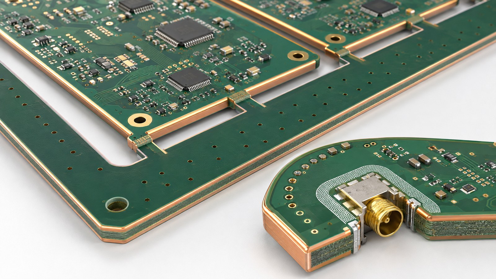
Edge plating requires access to the board edge, while production panels require material that holds the board during fabrication and assembly. A support tab placed through a functional plated segment interrupts the finished metal and can leave a rough breakout. A fully plated perimeter may therefore conflict with the proposed panel route.
The designer does not need to invent the factory panel, but should identify critical no-tab zones and acceptable break locations. The fabricator can then choose a routed panel, temporary support strategy or agreed interruptions compatible with its process.
| Panel concern | Possible result | Data needed |
| Tab crosses plated segment | Missing metal or rough witness after depanelization | Critical continuous zones and permitted breaks |
| Insufficient handling support | Board movement or process instability | Array drawing and assembly handling needs |
| Late profile revision | Copper and route no longer align | One released outline revision |
| Corner or cutout ambiguity | Unplated gap or unintended bridge | Enlarged edge detail and finish callout |
How Material, Thickness and Edge Geometry Affect Feasibility
Feasibility depends on the specific stackup, board thickness, copper construction, profile geometry and factory route. Straight external edges are generally easier to define and inspect than narrow internal cutouts, acute corners or small isolated plated segments.
Before quotation, ask the supplier to confirm the proposed edge feature against the released stackup. Items that may change the route include hybrid RF materials, very thin or thick boards, heavy outer copper, sequential structures, controlled-depth features and tight mechanical interfaces.
EBest Circuit’s exact limits for a particular edge-plated build should be treated as to be confirmed through the original capability data and project DFM review. Do not assume that a value used on one material, plant or special process applies to every order. The broader PCB design for manufacturability guide explains why stackup and profile constraints should be reviewed together.
Which Surface Finish Should Be Specified?
Select the finish from the electrical contact, solderability, durability, storage and system requirements—not from edge plating alone. A plated edge that only completes a shield boundary may have different wear requirements from a repeated mechanical contact.
- State whether the edge is a mating contact, solderable feature, enclosure interface or non-contact shield boundary.
- Identify any wear, corrosion, bonding or conductivity requirement.
- Confirm that the chosen finish can be applied consistently to the intended edge geometry.
- Keep connector fingers and their finish specification separate when they use a different construction.
- Define inspection expectations for coverage and exposed base copper.
For a general comparison of finish choices, use the PCB surface-finish selection guide. The final selection still requires project-specific confirmation.
What Gerber Layers and Fabrication Notes Should Show
A quote-ready package identifies the plated segments in both machine-readable artwork and a human-readable drawing. Do not rely on an email sentence after the data has been released.
- Provide Gerber, ODB++ or another agreed manufacturing dataset.
- Include one controlled board-profile layer with slots and cutouts.
- Show outer-layer copper reaching each intended plated edge.
- Show solder-mask openings associated with the feature.
- Label the electrical net and any deliberate breaks.
- Dimension critical contact zones, no-tab zones and mating locations.
- Specify surface finish and the expected finished appearance.
- Add a fabrication note such as “plate only the highlighted routed edges; all other edges remain unplated,” then reference the correct detail.
Include a neutral 3D image or PDF detail for communication if useful, but make the controlled fabrication data authoritative. The PCB fabrication specifications checklist can help organize the rest of the build package.
Which DFM Failures Cause Gaps, Peeling, Shorts or Rough Edges?
Most edge-plating failures begin as a disagreement among the electrical design, mechanical profile and panel route. Review the failure mechanism before changing only the visible copper artwork.
| Symptom | Likely question | Prevention |
| Gap in a critical segment | Did a tab, route transition or artwork break cross the edge? | Define continuous zones and review panel support |
| Unintended short | Was another net or connector feature too close to the plated route? | Run all-layer clearance and net checks |
| Peeling or weak adhesion | Does the copper construction and process support the geometry? | Confirm stackup and edge preparation with the fabricator |
| Rough breakout | Was a functional surface used as a depanelization point? | Move tabs or define an acceptable non-contact break |
| Finish does not cover as expected | Was the edge included in the finish and inspection callout? | State the finished condition and acceptance criteria |
How Should Edge Plating Be Inspected and Accepted?
Acceptance should address coverage, continuity, isolation, finish and mechanical interface. Visual appearance alone cannot prove the intended electrical function.
- Verify the correct edges and only those edges are plated.
- Inspect critical segments for gaps, exposed base material, blisters, peeling and rough damage.
- Check isolation from different-net copper and adjacent connector contacts.
- Measure continuity or resistance where the drawing defines an electrical requirement.
- Fit-check the enclosure, spring contact or gasket when the edge is a mechanical interface.
- Record first-article photographs of critical corners, breaks and contact zones.
- Agree in advance how permitted panel-break witness marks will be judged.
For RF hardware, functional verification may also include enclosure-level EMC or RF testing because a good-looking edge cannot compensate for gaps elsewhere in the shield or return path.
What Changes Edge-Plating Cost and Lead Time?
Cost and lead time depend on plated length and complexity, stackup, routing, panel support, finish, inspection and first-article requirements. Selective straight segments with clear data are easier to assess than a nearly continuous perimeter broken by connectors, tabs and internal cutouts.
Ambiguous data adds engineering exchanges and can delay quotation. A special panel strategy, unusual finish, tight contact tolerance or additional electrical/mechanical inspection can add setup and processing time. Ask suppliers to separate non-recurring engineering or tooling from recurring unit cost so quotes can be compared on the same assumptions.
What to Send for an Edge-Plating RFQ
The RFQ must let the supplier reconstruct the electrical, mechanical and manufacturing intent without guessing. Send:
- Gerber or ODB++ data, drill files and one authoritative board profile.
- Stackup, material selection, finished thickness and copper requirements.
- A drawing that highlights every plated segment and intentional break.
- The plated-edge net and its connection to planes or stitching vias.
- Solder-mask openings, connector keep-outs and enclosure contact zones.
- Permitted and prohibited panel-tab locations.
- Surface finish and any wear, bonding or corrosion requirement.
- Quantity, prototype or production stage and target delivery date.
- First-article, continuity, dimensional and visual acceptance requirements.
- BOM, CPL and assembly drawings when fabrication and assembly will be quoted together.
Label unresolved items as “supplier to confirm” rather than silently assuming a factory limit. That makes the DFM response part of the controlled engineering record.
FAQ About PCB Edge Plating
Is PCB edge plating the same as castellated holes?
No. Edge plating creates a conductive wrap along a routed edge, while castellated holes form solderable half-holes for board-to-board assembly. Their artwork and acceptance criteria differ.
Does edge plating always need to connect to ground?
No. Grounding is common for shielding and chassis interfaces, but the correct net follows the product architecture. State the intended net explicitly.
Can an entire PCB perimeter be edge plated?
Potentially, but production panel support and depanelization must still be solved. A nominally continuous perimeter may require agreed breaks or a special handling route.
Can edge plating improve EMC?
It can support a shorter, more continuous shielding or return path, but EMC performance depends on the entire enclosure, planes, via stitching, connectors and apertures.
Should copper extend to the board outline?
For intended edge-plated segments, outer-layer copper is typically designed to meet the finished route according to the fabricator’s data convention. Confirm the exact artwork rule during DFM.
Should solder mask cover a plated PCB edge?
A functional plated contact normally requires a coordinated mask opening. The correct opening depends on the intended contact and the supplier’s registration and process rules.
Why do panel tabs matter?
A tab can interrupt a plated segment and leave a rough witness after breakout. Mark critical no-tab zones and permitted breaks before the array is finalized.
Which surface finish is best for edge plating?
There is no universal choice. Select the finish from conductivity, wear, solderability, corrosion and mating requirements, then confirm it for the edge geometry.
How is edge plating inspected?
Inspection can include visual coverage, continuity, isolation, dimension and fit with the mating enclosure or contact. Define the required evidence in the drawing or quality plan.
What is the most important RFQ detail?
A marked fabrication detail showing exactly which edges are plated, their net, the finish and acceptable panel breaks. Without it, the supplier must guess at the core requirement.
Need a PCB quote with edge plating?
Send EBest Circuit your Gerber/ODB++ files, stackup, plated-edge drawing, net assignment, surface finish, panel constraints, quantity and acceptance requirements. We will review the project data and confirm the applicable manufacturing route before quotation.