A UHDI printed circuit board moves beyond conventional HDI when at least one critical feature enters the ultra-fine range. That change affects far more than trace width. The imaging method, copper build, microvia geometry, dielectric thickness, registration plan, solder mask, inspection criteria, and assembly interface must be treated as one manufacturing system.
This guide helps design and procurement teams decide whether a project is truly UHDI, where early DFM work prevents redesign, and what evidence should be agreed before prototype release. It also separates published working thresholds from a supplier’s confirmed production capability—an important distinction when yield, reliability, and repeatability matter.
What Is a UHDI Printed Circuit Board?
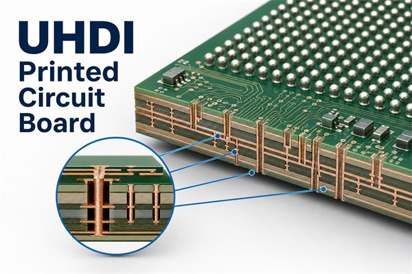
UHDI means ultra-high-density interconnect. The industry’s working definition generally places a board in UHDI territory when one or more features go beyond the highest conventional HDI producibility range. Common reference thresholds include:
- Conductor line width below 50 µm.
- Conductor spacing below 50 µm.
- Build-up dielectric thickness below 50 µm.
- Laser microvia diameter below 75 µm.
These figures are useful screening points, not permission to combine every minimum on one design. A board with 45 µm spacing on one layer may require a different process route from a board with 60 µm traces and 50 µm microvias. Material, copper thickness, panel format, feature distribution, registration tolerance, surface finish, and annual volume all affect the real production window.
The shorter phrase ultra hdi pcb often refers to the same technology. In practice, the fabrication drawing should state the actual features and acceptance requirements instead of relying on the label alone.
How Does UHDI Differ from Conventional HDI?
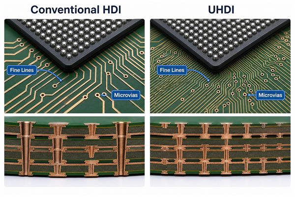
Conventional HDI gains density through laser microvias, blind or buried connections, sequential lamination, and via-in-pad. UHDI keeps those concepts but pushes selected geometries beyond conventional HDI process limits. That shift changes both the fabrication method and the amount of process verification required.
| Design Area | Conventional HDI | UHDI Consideration |
| Fine conductors | Often produced by optimized subtractive etching | May require mSAP, SAP, or another ultra-fine-line process |
| Microvias | Laser-drilled vias commonly around the 0.10 mm class | Smaller geometry needs tighter drilling, plating, and registration control |
| Dielectrics | Build-up films selected around a proven HDI stackup | Very thin dielectrics make copper balance and via aspect ratio more sensitive |
| Inspection | AOI, electrical test, impedance test, and microsection as specified | More detailed coupons, dimensional evidence, and agreed acceptance rules may be needed |
A designer should therefore ask, “Which features require UHDI?” rather than applying ultra-fine geometry across every layer. Restricting the most demanding rules to the package escape or other density-critical zones can improve yield and cost without sacrificing electrical performance.
HDI PCB Design Guidelines for UHDI Layouts
Useful hdi pcb design guidelines begin with the fabricator’s production window, not the CAD tool’s minimum setting. The following decisions should be closed before routing is frozen:
- Define the density driver. Record BGA pitch, pad diameter, escape count, available routing channels, and the layers that genuinely need ultra-fine features.
- Use regional rules. Keep wider traces and spaces outside dense package fields where possible. A mixed-rule design is usually easier to control than a board built entirely at the minimum.
- Separate line and space values. Do not assume a supplier’s minimum line width automatically permits the same minimum clearance after plating.
- Coordinate copper with geometry. Thicker copper is harder to resolve into very fine conductors. Base copper and final copper must both appear in the fabrication notes.
- Treat solder mask as a precision layer. Mask registration, dam width, pad definition, and via treatment can determine whether fine-pitch assembly is practical.
- Control impedance from the real stackup. Trace geometry, dielectric thickness, resin content, copper profile, and reference-plane distance must be reviewed together.
Do not design every feature at a supplier’s stated limit. The published minimum may describe a test coupon or a restricted build, while the stable production value may be wider. A useful DFM conversation distinguishes prototype feasibility, repeatable production, and the conditions attached to each.
HDI PCB Stackup Decisions for UHDI
An hdi pcb stackup cannot be finalized independently from the escape strategy. The number of build-up layers, microvia spans, plane assignment, material family, and impedance targets determine the lamination sequence and the inspection plan.
Review these points together:
- Build-up architecture: confirm whether 1+N+1, 2+N+2, any-layer, or another construction is actually required.
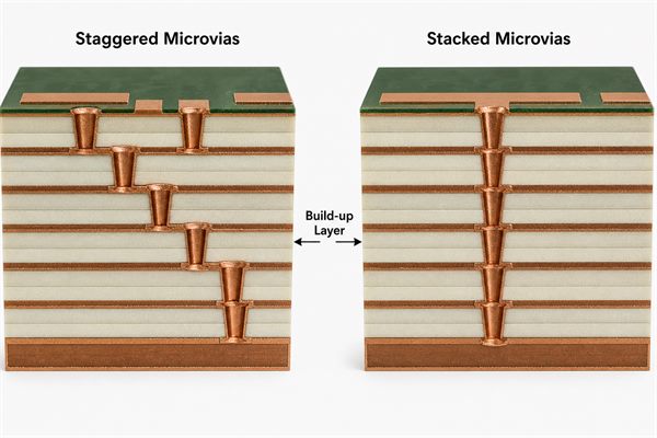
- Microvia type: use staggered microvias where routing permits; specify stacked structures only where density justifies the additional process and reliability burden.
- Via aspect ratio: match microvia diameter to dielectric depth. A small opening through an unnecessarily deep dielectric creates plating risk.
- Via fill and cap: via-in-pad normally requires a defined fill, planarization, and cap-plating sequence before component assembly.
- Stack symmetry: balance copper and dielectric construction to reduce bow, twist, and registration drift through repeated thermal cycles.
- Material availability: confirm the exact laminate, build-up film, copper foil profile, thickness tolerance, and approved substitutes before impedance values are released.
Early stackup review is especially important when UHDI routing is combined with high-speed interfaces. Our existing guide to HDI PCB structures explains conventional 1+N+1, 2+N+2, and every-layer interconnect concepts, while the separate 80 GHz UHDI PCB article focuses on RF material and impedance concerns.
How Does the HDI PCB Manufacturing Process Change for UHDI?
The hdi pcb manufacturing process normally uses sequential build-up, laser drilling, copper deposition, imaging, plating, lamination, and electrical verification. UHDI adds tighter interactions between these steps and may change the conductor-forming method.
- Engineering review: identify every sub-50 µm feature, microvia span, impedance structure, copper requirement, and inspection coupon.
- Material and process selection: choose a laminate, build-up dielectric, copper foil, and imaging route that can hold the requested geometry.
- Core and build-up imaging: form fine conductors with a process selected for the target line, space, and copper thickness.
- Laser drilling and desmear: control via diameter, taper, landing accuracy, and the condition of the target pad.
- Metallization and filling: establish reliable copper in the microvia, fill specified structures, and planarize via-in-pad surfaces.
- Sequential lamination: repeat build-up cycles while controlling registration, resin flow, copper balance, and thickness.
- Surface formation: apply solder mask and surface finish without consuming the clearances needed for fine-pitch assembly.
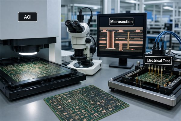
- Inspection and test: use AOI, electrical testing, microsection, dimensional measurement, impedance testing, or other project-specific evidence.
Subtractive etching can support some near-UHDI geometries, but very fine and consistent conductors may require modified semi-additive or semi-additive processing. The correct route depends on feature size, copper thickness, layer location, panel scale, volume, and supplier capability. It should be confirmed before the layout is locked.
Which DFM Risks Cause UHDI Prototype Failure?
UHDI prototypes most often become expensive when a local density decision triggers an unplanned process change. The risk is rarely one number in isolation.
- Minimum geometry used everywhere: reduces the process margin across the whole panel even though only a small BGA area needs it.
- Excessive stacked microvias: increases lamination count and concentrates thermo-mechanical stress.
- Unconfirmed copper build: fine lines may not survive the plating and etching sequence at the requested final copper.
- Ambiguous via notes: missing fill, cap, target-layer, or aspect-ratio requirements can change both cost and reliability.
- Late impedance modeling: forces trace-width or dielectric changes after routing is complete.
- Insufficient mask clearance: causes assembly constraints even when the copper pattern can be fabricated.
- No agreed acceptance plan: leaves the customer and supplier evaluating fine features with different criteria.
A strong DFM response should show what must change, why it matters, and whether the recommendation affects electrical performance. “Cannot build” is not enough; the customer needs an alternative feature, stackup, or process route.
What Inspection Evidence Should Be Defined?
Electrical continuity alone cannot prove that a UHDI process is stable. The inspection plan should follow the critical risks in the design and may include:
- AOI coverage for fine-line layers.
- Microsection locations that represent stacked or staggered microvias.
- Measurement of finished line width, spacing, dielectric thickness, and via geometry.
- Impedance coupons that match the controlled layers and copper construction.
- Electrical test coverage and netlist source.
- Surface-finish thickness or wire-bond acceptance criteria when applicable.
- Assembly X-ray or other inspection for fine-pitch packages when the project includes PCBA.
At EBest Circuit, our documented quality resources include AOI, electrical testing, impedance testing, microsection inspection, copper-thickness testing, 2D measurement, and X-ray inspection for relevant assembly work. The final test plan still depends on the product, customer specification, and confirmed process route. See our PCB quality and testing overview for the broader control framework.
How Do UHDI Choices Affect Cost and Lead Time?
UHDI does not automatically make the lowest system cost, even when it reduces board area. Cost and lead time rise when a design adds specialized material, semi-additive conductor formation, more lamination cycles, stacked microvias, tight registration, extra coupons, or low-yield feature combinations.
The practical cost levers are:
- How many layers actually need ultra-fine line and space.
- Whether a standard panel and material construction can be used.
- The number of sequential lamination cycles.
- Staggered versus stacked microvia architecture.
- Base and finished copper thickness.
- Surface finish and fine-pitch assembly requirements.
- Prototype quantity, test evidence, and volume forecast.
A compact UHDI board can still lower total product cost when it removes connectors, reduces board area or layer count, shortens critical interconnects, or enables a smaller enclosure. The comparison should therefore use total system impact, not PCB unit price alone.
What Should Be Included in a UHDI RFQ Package?
Provide enough information for the supplier to evaluate the exact feature combination. A useful package includes:
- Gerber or ODB++ fabrication data and the fabrication drawing.
- Proposed layer stackup, material family, finished thickness, and copper weights.
- A list of the minimum line, minimum spacing, smallest microvia, and affected layers.
- Microvia spans, stacked or staggered structure, via fill, and cap-plating notes.
- Controlled-impedance table and reference-layer information.
- Surface finish, solder mask, legend, and assembly constraints.
- Test standard, inspection evidence, coupon requirements, and acceptance class.
- Prototype quantity, expected annual volume, and requested delivery date.
- BOM, pick-and-place data, and assembly drawing when PCBA is required.
For a general supplier overview, you can also review our existing UHDI PCB fabrication page. Its purpose is supplier selection, while this page is intended to help engineering teams prepare a manufacturable design package.
FAQ About UHDI Printed Circuit Boards
Is every board with microvias a UHDI PCB?
No. Microvias are common in conventional HDI. UHDI is associated with one or more features beyond conventional HDI thresholds, such as sub-50 µm lines or spaces, sub-50 µm build-up dielectrics, or microvias below the 75 µm range.
Does UHDI always require mSAP?
No. The conductor-forming method depends on the target geometry, copper thickness, layer, panel, and supplier. Some near-UHDI features may be possible with advanced subtractive control, while tighter and more uniform conductors may need mSAP or SAP.
Are stacked microvias better than staggered microvias?
Not automatically. Stacked microvias save routing area, but they add process complexity and reliability sensitivity. Use them where density requires them; use staggered structures where the layout allows a more forgiving construction.
Can standard HDI design rules be reused for UHDI?
They are a starting point, not a release condition. UHDI requires a supplier-specific review of fine-line formation, dielectric depth, via geometry, copper build, registration, solder mask, inspection, and production volume.
How Can EBest Circuit Review Your UHDI Project?
EBest Circuit has provided PCB and PCBA support since 2006. We work with customers on PCB design review, prototyping, multilayer and HDI fabrication, component sourcing, assembly, and testing. Our documented management and compliance resources include ISO 9001:2015, ISO 13485:2016, IATF 16949, AS9100D, UL, RoHS, and REACH; applicability should be confirmed for the specific product and production route.
For a true UHDI request, we do not treat a marketing label as a capability approval. Our team first reviews the line and space by layer, dielectric construction, microvia geometry, copper build, stackup, impedance, surface finish, quantity, and required evidence. We then confirm whether the project fits an available process route or needs design adjustment. You can also review our broader PCB manufacturing capability information.
Send your Gerber or ODB++ files, stackup, impedance table, fabrication drawing, quantity, and test requirements to sales@bestpcbs.com. We will help identify the density-critical features, return practical DFM feedback, and confirm a manufacturable path for your UHDI printed circuit board before quotation.
You may also like




Tags: hdi pcb design guidelines, hdi pcb manufacturing process, hdi pcb stackup, UHDI printed circuit board, ultra hdi pcb