





Different PCB via types affect layer transitions, routing density, fabrication complexity, drill strategy, impedance behavior, and assembly yield. A simple 4-layer industrial control board may only need standard through vias, while a fine-pitch BGA or high-speed communication board may require microvias, via-in-pad, or backdrilling.
What Are PCB Vias?
A PCB via is a plated hole or laser-formed interconnection that electrically connects copper features on different layers of a printed circuit board. Vias let signals, power, and ground move between layers when routing cannot stay on one surface.
In a low-density design, vias are mainly a routing convenience. In a dense or high-speed design, the via structure becomes an engineering decision that affects stackup planning, manufacturability, cost, reliability, and electrical performance.
The most important thing to remember is that a via is not just a hole. It also brings pad size, drill tolerance, annular ring, aspect ratio, anti-pad size, plating quality, and sometimes resin filling or copper capping into the design decision.
Main PCB Via Types
The most common way to classify vias is by how many layers they connect and how they are manufactured.
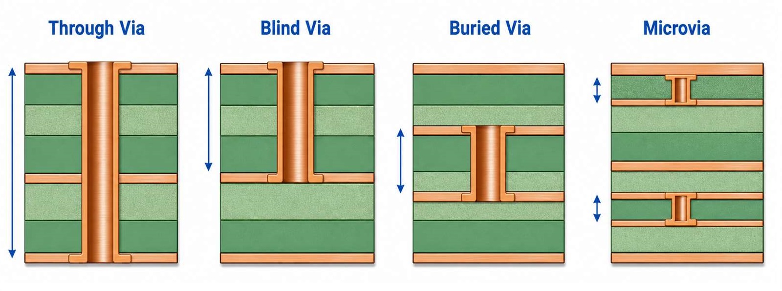
Common PCB via types used in multilayer and HDI designs.
| Via Type | Connects | Typical Use | Relative Cost | Main Limitation |
|---|---|---|---|---|
| Through hole via | Top to bottom through full board | General routing, power, standard multilayer PCBs | Lowest | Occupies space on every layer |
| Blind via | Outer layer to one or more inner layers | Higher routing density, partial layer transition | Medium to high | More complex lamination and drilling |
| Buried via | Inner layer to inner layer only | Dense multilayer routing | High | Cannot be accessed from outer layers |
| Microvia | Usually laser-drilled between adjacent layers | HDI boards, fine-pitch BGAs, compact modules | High | Limited depth and tighter process window |
| Via in pad | Via placed directly in component pad | Fine-pitch BGA escape routing | High | Usually needs filling and plating |
| Backdrilled via | Standard via with unused stub removed | High-speed signal integrity improvement | Medium to high | Extra fabrication step |
In practice, through vias handle most conventional boards. Blind, buried, and microvias are usually selected when routing density or package pitch justifies the added process cost.
Through Hole Vias
Through hole vias run from the top layer to the bottom layer and pass through the entire PCB thickness. They are the standard via type used in most commercial and industrial boards.
Their main advantage is cost efficiency. Fabricators can drill and plate them using conventional mechanical processes, and engineers can route between many layers without needing sequential lamination.
They also have clear limits:
- They consume routing space on every layer, even when the signal only needs a short layer transition.
- They create via stubs on unused portions of the hole, which can hurt high-speed performance.
- They are less efficient under fine-pitch BGAs because the drill and pad consume too much real estate.
For standard boards, through vias are still the default choice because they are easy to quote, easy to fabricate, and usually the most reliable from a process standpoint.
Blind and Buried Vias
Blind vias start on an outer layer and end on one or more inner layers. Buried vias connect only inner layers and are invisible from the outside surfaces after lamination.
They are mainly used when a through via would waste too much routing area or block breakout under dense packages.
Different via depths support different routing and stackup goals.
| Factor | Blind Via | Buried Via |
|---|---|---|
| Visible from surface | Yes | No |
| Routing benefit | Frees space on part of the board | Frees surface space completely |
| Typical board type | Dense multilayer digital or RF boards | High-layer-count dense routing boards |
| Process complexity | Sequential lamination or controlled drill depth | Inner-layer build-up before final lamination |
| Cost impact | Significant | Significant to high |
A blind or buried via structure should be chosen because the board actually needs the routing density, not because it sounds more advanced. If a standard stackup and through-via escape can already meet spacing and signal needs, blind or buried vias often add cost without enough return.
Microvias and HDI PCB Design
Microvias are very small vias, usually laser drilled, and most often connect adjacent layers such as L1-L2 or L2-L3 in an HDI PCB stackup. They are common in smartphones, wearable devices, camera modules, communication equipment, and fine-pitch BGA designs.
Microvias are often used under fine-pitch BGA areas to improve fanout density.
Microvias are useful because they take much less surface area than mechanical vias, which makes breakout routing under fine-pitch packages much easier. They also reduce via stub length and can improve electrical behavior when designed correctly.
But they come with real process boundaries:
- They usually connect only adjacent layers unless stacked or staggered structures are used.
- Stacked microvias increase process risk if plating quality is not tightly controlled.
- They require HDI-capable fabrication, which raises cost and lead time.
- They need closer coordination between stackup design, drill plan, and copper thickness.
If the design uses fine-pitch BGA packages, very high I/O counts, or compact form factors, microvias may be necessary. If not, they can be an expensive over-design choice.
Via in Pad and Filled Vias
Via in pad means the via is placed directly in the pad of a component, most often under a BGA. This is common when the package pitch is too tight for dog-bone fanout with standard vias.
Via-in-pad structures usually require extra processing such as resin filling, conductive or non-conductive via fill, copper capping or planarization, and flat pad surface control for assembly.
Without proper filling, solder can wick into the hole during reflow, which creates poor solder joints and assembly defects.
For that reason, via-in-pad is not just a layout option. It is also a fabrication and assembly choice that must be confirmed in the quotation stage. If the supplier cannot support filled and capped vias consistently, the yield risk rises quickly.
Backdrilled Vias for High-Speed PCB Design
Backdrilling removes the unused drilled barrel portion of a through via after plating. The purpose is to reduce via stub length, which helps high-speed signals by lowering unwanted reflections and impedance discontinuities.
Backdrill is most relevant when the board includes high-speed differential pairs, long backplane or connector channels, SerDes links, or network, server, telecom, and high-speed computing hardware.
Backdrilling removes the unused via stub when signal integrity requires it.
It is usually unnecessary for low-speed control boards, ordinary power products, or designs where stub length is not a signal integrity problem. Backdrilling should be driven by channel performance needs, not added by default.
How to Choose the Right Via Type
The best via type depends on routing density, package pitch, board thickness, signal speed, cost target, and fabrication capability.
| Design Need | Usually Best Choice |
|---|---|
| Standard industrial or consumer multilayer PCB | Through hole via |
| Moderate routing density with outer-layer congestion | Blind via |
| Dense inner-layer routing in multilayer board | Buried via |
| Fine-pitch BGA or compact HDI design | Microvia |
| Extremely tight BGA breakout | Via in pad |
| High-speed channel with harmful via stubs | Backdrilled via |
A good selection workflow is: start with the simplest via structure the board can support, check whether package breakout, spacing, and layer count still work, and escalate only when the design actually needs it.
PCB Via Design Rules That Matter
Even when the via type is correct, poor via geometry can still create yield or reliability problems. The most common design items to review are finished hole size, pad size and annular ring, aspect ratio, anti-pad clearance in reference planes, copper-to-hole clearance, via-to-via spacing, tenting or filling requirements, and drill-to-copper registration tolerance.
For conventional mechanical vias, aspect ratio is one of the first manufacturing filters. If the board gets too thick relative to the drill size, plating quality becomes harder to control. For HDI microvias, the key concern shifts more toward laser drill quality, copper fill reliability, and stacked-via robustness.
Cost Impact of Different Via Types
Via choice can change the PCB price materially, especially when the board moves from standard multilayer fabrication into HDI processing.
| Via Type | Cost Impact Driver |
|---|---|
| Through hole via | Standard drill and plate process |
| Blind via | Sequential lamination, extra drill control |
| Buried via | Inner-layer sub-build and extra lamination |
| Microvia | Laser drilling, HDI build-up process |
| Via in pad | Filling, planarization, tighter assembly control |
| Backdrill | Additional drill step and registration control |
If a project is still in prototype or cost-down review, it is worth asking whether the same routing goal can be achieved by adding one more signal layer, adjusting BGA fanout strategy, changing stackup, reassigning pin escape, or using a slightly larger board outline.
What to Provide When Requesting a Quote for PCB Via Structures
A useful quotation needs more than Gerber files when advanced vias are involved. The supplier should know exactly which via structures are required and which ones are optional.
Customers should provide:
- Gerber files or ODB++
- Layer stackup
- Drill file
- Via type requirements
- Filled or capped via notes, if needed
- Controlled impedance requirements
- BGA pitch or dense component details
- Board thickness and copper weight
- Reliability or test requirements
- Prototype quantity and production forecast
If the board includes blind vias, buried vias, microvias, via in pad, or backdrill, those details should be called out clearly in fabrication notes. Otherwise, the quote may assume a simpler process than the design actually needs.
How EBest Circuit Supports PCB Via Design and Manufacturing?
EBest Circuit, also known as Best Technology, supports standard multilayer PCB fabrication as well as more advanced PCB and PCBA projects that involve dense routing, DFM review, and stackup planning.
For engineers, the most useful support is usually early manufacturability review. The team can help check whether a via structure is necessary, whether the drill plan is realistic, and whether a routing target can be simplified before the design reaches fabrication.
That matters most when the project involves:
- Fine-pitch BGA breakout
- HDI stackups
- Blind or buried via decisions
- Via in pad requirements
- Prototype-to-production transfer
Because EBest Circuit integrates PCB manufacturing, component sourcing, assembly, and engineering support, the discussion can stay focused on real tradeoffs between manufacturability, cost, and delivery rather than just a bare-board drawing review.
Conclusion
Understanding PCB via types is really about understanding tradeoffs. Through vias are the standard choice for most boards. Blind and buried vias help when routing density rises. Microvias and via in pad become important in HDI and fine-pitch BGA work. Backdrilled vias matter when signal speed makes via stubs a real problem.
The right decision is usually the simplest via structure that still meets routing, electrical, and manufacturing requirements. If you are evaluating via structures for a new PCB or PCBA project, contact EBest Circuit at sales@bestpcbs.com for DFM review and quotation support.
You may also like



Tags: backdrill via, buried via pcb, microvia pcb, through hole vs blind via, types of vias in pcb, via in pad pcb