

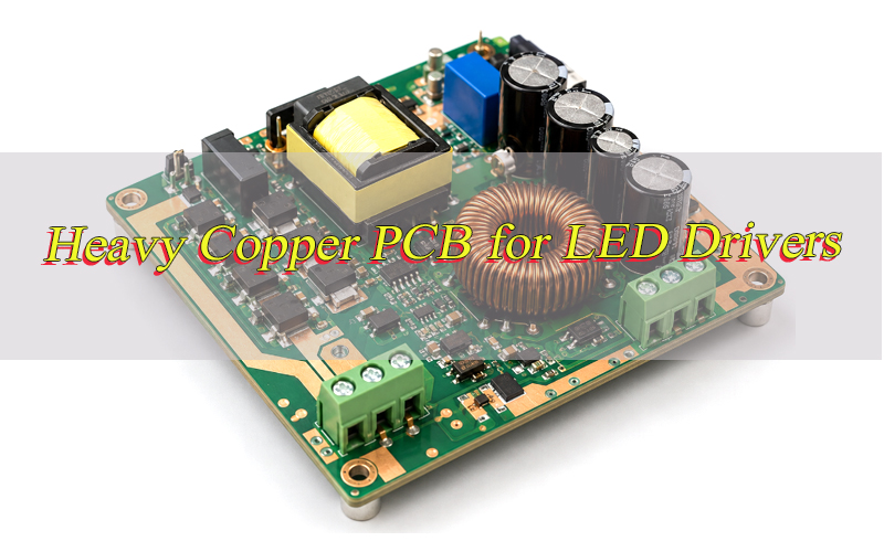
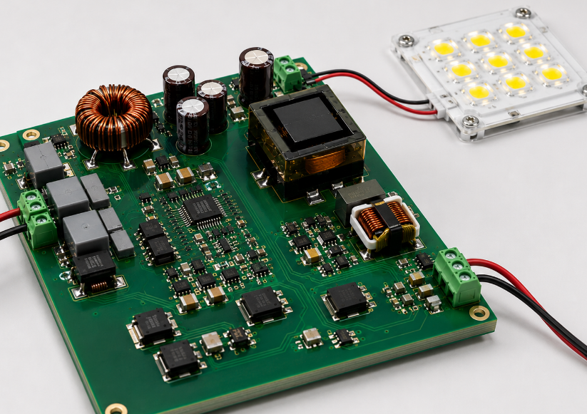
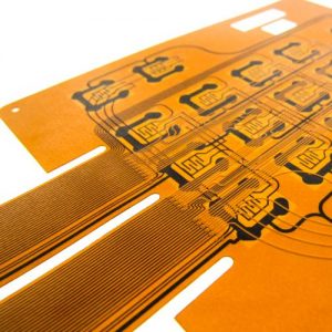
Heavy copper PCB for LED drivers is used when a driver board must carry higher current, control heat and stay stable during long operating hours. In LED power supply designs, MOSFETs, rectifiers, inductors, transformers, terminals and output current paths can create concentrated heat, so the board requires stronger copper, wider current paths and controlled thermal design.
For LED street lights, industrial lamps, UV LED systems and grow lights, heavy copper PCB for LED drivers helps improve driver output stability, temperature control and service life. This guide explains copper thickness, stackup, high-current routing, thermal vias, materials, manufacturing limits, testing, cost factors and supplier selection for heavy copper PCB for LED drivers.
Why Use Heavy Copper PCB for LED Drivers?
Heavy copper PCB for LED drivers improves current capacity, reduces copper loss and spreads heat more effectively than standard copper boards. LED drivers convert, regulate and protect power before sending stable current to LEDs, so the PCB becomes part of the electrical and thermal system.
In high-power lighting, current paths around MOSFETs, diodes, inductors, transformers and output terminals can become heat sources. Thick copper reduces resistance, helps control voltage drop and improves thermal stability. For LED street lights, industrial lighting, UV LED systems and high-current LED modules, heavy copper PCB for LED drivers gives the power section more safety margin before long-term operation.
What Problems Do Standard PCBs Face in LED Driver Applications?
Standard PCBs can face overheating, excessive voltage drop, narrow current bottlenecks and shorter service life in high-power LED driver applications. A 1 oz copper board may handle control signals, but it can become weak when the same board carries high current for long periods.
Common risks include hotspots near power components, overheated output traces, weak plated holes, solder joint fatigue and unstable driver output. Compact LED driver layouts often leave limited room for wide traces. If copper thickness is too low, the layout may require very wide copper areas that do not fit the available board size.
For high-power lighting products, heavy copper PCB for LED drivers gives the power section more margin against current overload, trace heating and long-hour thermal stress. This is especially useful when the driver board has compact space, dense components or limited airflow inside the enclosure.
How Does Heavy Copper PCB Improve LED Driver Thermal Management?
Heavy copper spreads heat through larger copper mass and lowers I²R loss in power paths. LED driver thermal management depends on both heat generation and heat transfer. Lower copper resistance reduces heat created by the current path itself.
At the same time, copper planes can move heat away from MOSFETs, rectifiers and current sense areas. In real LED driver thermal management, heavy copper PCB must work together with component placement, short current loops, thermal vias, copper pours, heat pads and a clear path to the enclosure, heat sink or airflow area.
In practical LED power supply projects, heavy copper PCB for LED drivers should be considered early in the layout stage, not after the circuit is finished. When copper weight, trace width and heat-spreading areas are planned together, the board is easier to test, assemble and scale into mass production.
What Copper Thickness Is Suitable for LED Driver PCB Design?
Most LED driver PCB designs use 2 oz to 4 oz copper, while 3 oz copper is a common balance between current capacity, manufacturability and cost. Higher copper thickness may be selected when current is high, board area is limited or temperature rise must be tightly controlled.
| Copper | Common Use | Notes |
|---|---|---|
| 1 oz | Low-power control area | Not ideal for high-current output paths |
| 2 oz | Medium-power LED drivers | Better current and thermal margin |
| 3 oz | High-current LED driver boards | Common heavy copper choice |
| 4 oz | High-power LED power supply PCB | Stronger current capacity |
| 5 oz+ | Special power modules | Higher cost and tighter DFM control |
A 3oz copper PCB for LED driver projects is often a practical starting point, but the final value should be selected with current, trace width, allowable temperature rise, board size, copper area, via structure and assembly method.
For many medium-to-high-power lighting projects, heavy copper PCB for LED drivers starts with 2 oz or 3 oz copper, then moves to 4 oz or higher when current density, board size or temperature rise becomes more demanding.
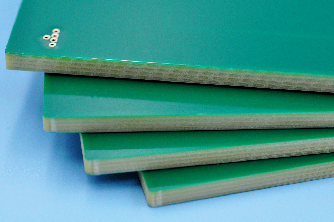
How Should a Heavy Copper PCB Stackup Be Designed for LED Drivers?
A heavy copper PCB stackup for LED drivers should separate high-current power paths, ground reference, thermal spreading and control signals. The stackup depends on driver power, board size, current level, heat source location and routing density.
For simple LED driver boards, a 2-layer heavy copper PCB is often enough. The top layer can carry power components and high-current routing, while the bottom layer provides wider copper areas for return current and heat spreading.
| Stackup | Layer | Copper | Function |
|---|---|---|---|
| 2-layer | L1 | 2 oz–4 oz | Components, input/output power routing, MOSFET area |
| 2-layer | L2 | 2 oz–4 oz | Ground return, heat spreading, large copper plane |
For higher-power or compact LED drivers, a 4-layer stackup gives better separation between power and control circuits. It also improves grounding and reduces routing congestion.
| Stackup | Layer | Copper | Function |
|---|---|---|---|
| 4-layer | L1 | 2 oz–4 oz | Power components, high-current routing, thermal copper |
| 4-layer | L2 | 1 oz–2 oz | Ground plane, return path, noise control |
| 4-layer | L3 | 1 oz–2 oz | Power plane, auxiliary power or control routing |
| 4-layer | L4 | 2 oz–4 oz | Output routing, bottom heat spreading, terminals |
A mixed copper stackup can reduce cost when only part of the LED driver carries high current. For example, the outer layers can use 3 oz copper for power routing, while inner layers use 1 oz or 2 oz copper for ground, control and auxiliary circuits. This LED driver PCB stackup heavy copper approach is useful when MOSFETs, transformers, current sense resistors, terminals and control ICs share one board.
A practical stackup for heavy copper PCB for LED drivers should keep high-current layers close to the main power components and provide a stable return path through ground or power planes. This helps reduce current loop area, thermal rise and switching noise.
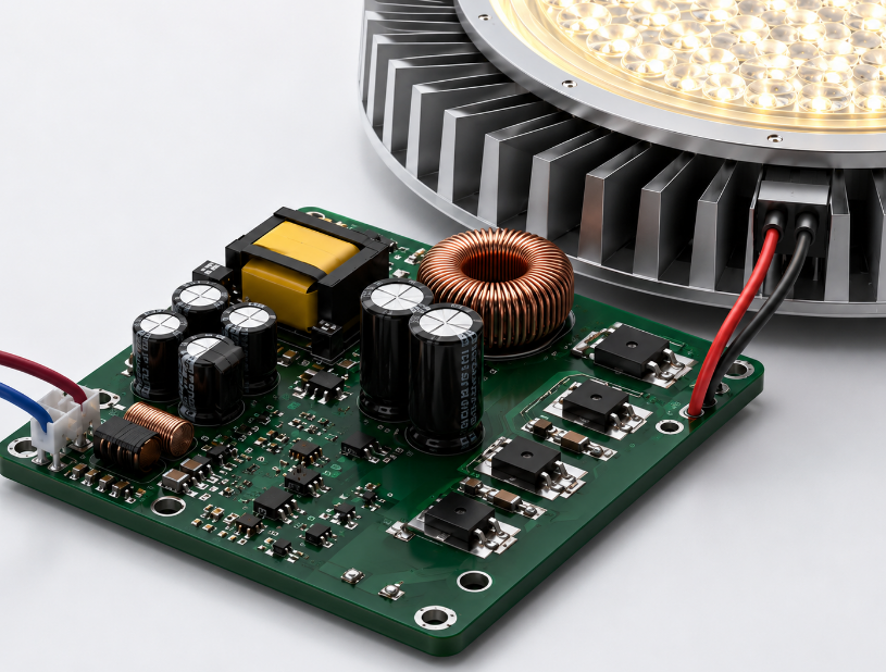
When Should You Choose Heavy Copper PCB Instead of Aluminum PCB for LED Drivers?
Choose heavy copper PCB when the LED driver has high-current paths, complex routing, multilayer circuits or mixed SMT and through-hole components. Aluminum PCB is better for LED light source boards, while heavy copper PCB is usually better for driver power circuits.
- Choose heavy copper PCB when the board includes MOSFETs, transformers, bridge rectifiers, inductors, terminals, protection circuits and control ICs.
- Use heavy copper PCB when the LED driver requires 2-layer or 4-layer routing, not only a simple single-sided thermal path.
- Select heavy copper PCB when high-current input and output paths must be routed with wide copper, copper pours and controlled return paths.
- Use aluminum PCB when the main task is transferring heat from LED chips to a metal base.
- For many lighting products, the practical structure is: LED light board uses aluminum PCB, while the LED driver board uses heavy copper PCB.
This choice keeps the light source board focused on LED heat transfer and the driver board focused on power conversion, protection and current control. For a heavy copper board for high power LED systems, this separation can also make testing, troubleshooting and replacement easier.
How to Design High Current Traces for LED Driver PCBs?
High current PCB for LED drivers should use short, wide and direct copper paths to reduce resistance, voltage drop and heat concentration. The power loop should be planned before small signal routing, because current path quality directly affects temperature rise and driver stability.
- Keep the main current path from input terminal, rectifier, MOSFET, inductor, capacitor and output terminal as short as possible.
- Use wide traces or copper pours for high-current input, switching and output sections.
- Avoid narrow necks between pads, vias, terminals and copper planes, because these areas often become hotspots.
- Use multiple vias when current must move between layers, and place them close to the current path.
- Separate high-current switching areas from control ICs, feedback lines, dimming signals and sensing circuits.
- Keep creepage and clearance suitable for the working voltage, especially for AC input and isolated LED power supply designs.
- Review trace width with current, copper thickness, board temperature, airflow and enclosure conditions.
For high power LED driver circuit PCB layout, the target is not only carrying current. The board should also keep temperature rise, voltage drop and switching noise under control.
How Should Thermal Vias and Copper Areas Be Used in LED Driver PCB Layout?
Thermal vias and copper areas should form a continuous heat path from hot components to larger copper planes, bottom copper or external heat-dissipation structures. They are useful around MOSFETs, rectifiers, power resistors, regulators and thermal pads.
- Place thermal vias near heat-generating pads, but avoid weakening solder joints or creating solder wicking problems.
- Use via arrays instead of relying on one large via, because multiple vias spread heat more evenly.
- Connect thermal vias to bottom copper, internal ground planes or heat-spreading copper areas.
- Use large copper pours around power components, but keep copper balance suitable for soldering and board flatness.
- Avoid isolated copper islands, because they may store heat without transferring it away.
- Combine thermal vias with heat pads, copper planes, airflow, heat sinks or metal enclosures when the driver power is high.
- Review thermal via size, hole copper and spacing during DFM to avoid plating and soldering issues.
Thermal vias work best when they are part of the early stackup and heat path plan. Adding vias after layout completion may improve the drawing, but it often misses the real heat transfer route.
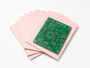
What Materials and Surface Finishes Work Best for Thick Copper LED Power Supply PCB?
Thick copper PCB for LED power supply projects usually uses FR4, High Tg FR4 or other heat-resistant laminates, depending on operating temperature and reliability targets. High Tg material is helpful when the board works near heat sources or faces thermal cycling.
| Item | Common Choice | Use Case |
|---|---|---|
| Base material | FR4 | Standard LED driver boards |
| High-temperature material | High Tg FR4 | Higher operating temperature |
| Copper | 2 oz–4 oz | Common LED driver range |
| Surface finish | HASL lead-free | Cost-sensitive power boards |
| Surface finish | ENIG | Fine pads and stable solderability |
| Protection | Conformal coating | Outdoor or humid lighting products |
Surface finish should match pad size, assembly method, storage time and environmental exposure. Outdoor LED drivers may also require coating compatibility, stable insulation distance and resistance to humidity or temperature cycling.
What Manufacturing Challenges Exist in Heavy Copper PCB for LED Drivers?
Heavy copper PCB for LED drivers is harder to manufacture than standard PCB because thick copper affects etching, lamination, solder mask and hole reliability. These issues should be checked before prototype and mass production.
- Thick copper requires stronger etching control, otherwise trace width and spacing may shift from the design value.
- Narrow spacing with thick copper increases the risk of copper residue, shorts or poor edge definition.
- Large copper areas may cause resin filling difficulty during lamination.
- Uneven copper distribution can increase board warpage or panel stress.
- Solder mask coverage is more difficult around thick copper edges, especially near dense pads.
- Plated through holes must have stable copper thickness to handle current and mechanical stress.
- Heavy copper pads absorb more heat during assembly, so soldering profiles and thermal relief design must be checked.
- Mixed copper designs require careful balance between high-current areas and fine signal routing areas.
For heavy copper PCB for LED drivers, manufacturability is part of reliability. In mass production, heavy copper PCB for LED drivers should be reviewed as both a power board and a thermal component. A reliable manufacturer should review copper spacing, hole structure, solder mask bridge, thermal relief, copper balance and panel design before production.
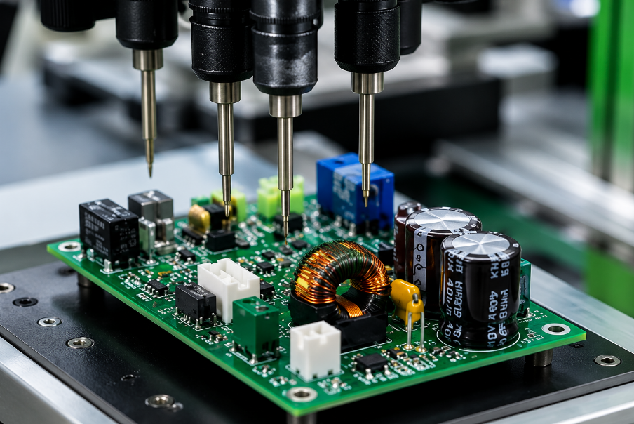
How Should Heavy Copper PCB Prototypes for LED Drivers Be Tested?
A heavy copper PCB prototype for LED projects should be tested step by step before mass production to confirm current capacity, solderability, thermal behavior and manufacturing stability.
First, the factory should review Gerber files, stackup, copper thickness, minimum trace spacing, drill size, hole copper, surface finish and panel design. This step helps find manufacturing risks before fabrication starts.
Second, after fabrication, the prototype should pass visual inspection, AOI and electrical testing. These checks confirm that there are no open circuits, short circuits, serious etching defects or surface finish problems.
Third, copper thickness and hole quality should be checked when the board carries high current. Microsection inspection can confirm plated hole reliability and copper distribution.
Fourth, the prototype should go through trial assembly. This helps check soldering behavior, large copper pad heat absorption, through-hole component fit and terminal strength.
Finally, the assembled LED driver should be tested under working load. Thermal rise, output stability, voltage drop and hotspot location should be reviewed before approving batch production.
What Quality Tests Are Important for High Power LED Driver PCBs?
High power LED driver PCBs should be tested for copper quality, electrical safety, solderability, hole reliability and thermal performance. These tests reduce field failure risk in lighting products that operate for long hours.
- AOI inspection checks trace defects, pad defects, copper residue and open circuit risks.
- Electrical test confirms that the PCB has no open circuits or short circuits before assembly.
- Copper thickness inspection verifies whether the board meets the required 2 oz, 3 oz, 4 oz or higher copper specification.
- Microsection inspection checks plated through hole quality, hole wall copper and lamination condition.
- Solderability testing confirms whether SMT pads, through-hole pads and terminals can be soldered reliably.
- Hi-pot testing is important for LED power supply boards with high voltage or isolation requirements.
- Thermal rise testing checks whether hotspots stay within the acceptable range under real working load.
- Visual inspection confirms solder mask coverage, surface finish quality, board edge condition and marking accuracy.
- Conformal coating inspection may be required for outdoor LED drivers, humid environments or industrial lighting projects.
For heavy copper PCB for LED drivers, quality testing should cover both electrical function and long-term thermal reliability. A board that passes basic continuity testing still requires current-path and heat-related checks before high-power use.
How Much Does Heavy Copper PCB Price for LED Driver Projects Depend On?
Heavy copper PCB price for LED driver projects depends on copper thickness, layer count, board size, trace spacing, hole density, material, testing and delivery time. Copper weight is usually one of the biggest cost drivers because it affects raw material use and fabrication difficulty.
Cost also rises when the design uses fine spacing with thick copper, dense vias, High Tg material, ENIG finish, strict testing or fast lead time. To control cost, keep high-current copper only where it is required, avoid unnecessary ultra-thick copper and confirm manufacturable spacing early. A good DFM review can reduce redesign and prototype waste.
The price of heavy copper PCB for LED drivers should be evaluated together with product reliability, not only the unit PCB cost. If a thicker copper design reduces overheating, redesign, rework or field failure risk, it may lower the total project cost.
How to Choose a Heavy Copper PCB Manufacturer for Lighting Applications?
Choose a heavy copper PCB manufacturer for lighting that can help you reduce design risk, control production quality and shorten communication time. For LED driver projects, the supplier should understand both PCB fabrication and real power board application issues.
- Check heavy copper capability first. The factory should support 2 oz, 3 oz, 4 oz or higher copper and understand how thick copper affects line width, spacing, plating, solder mask and assembly.
- Ask for DFM review before production. A good manufacturer should check copper spacing, stackup, hole copper, thermal vias, creepage, clearance and solder mask design before building the board.
- Confirm lighting and power PCB experience. LED driver boards usually include MOSFETs, transformers, rectifiers, inductors, terminals and control circuits, so general PCB experience is not enough.
- Review testing capability. Copper thickness inspection, microsection, electrical test, solderability check and visual inspection help reduce batch failure risk.
- Check prototype-to-mass-production support. A supplier that can support both samples and volume production helps you avoid supplier changes after design approval.
- Evaluate assembly support if needed. If your project includes BOM sourcing, SMT, through-hole assembly and testing, turnkey support can reduce purchasing workload and schedule risk.
- Compare communication quality, not only price. Fast engineering feedback, clear file review and practical suggestions often save more cost than a slightly lower board price.
The best supplier is not simply the cheapest one. For heavy copper PCB for LED drivers, the right manufacturer should help you prevent overheating, current-path failure, soldering issues and production delays before they become expensive problems.
Why Choose EBest for Heavy Copper PCB for LED Drivers?
EBest helps customers turn heavy copper LED driver PCB designs into manufacturable, testable and assembly-ready boards. As a China source factory serving global customers, we focus on practical support for lighting, power supply and high-current PCB projects.
- Design review before production. We can check copper thickness, stackup, trace spacing, high-current routing, thermal vias and manufacturability based on your Gerber files.
- Heavy copper PCB fabrication support. EBest can support LED driver boards using common heavy copper requirements such as 2 oz, 3 oz and 4 oz copper, depending on the project design.
- Lower trial-and-error risk. Early DFM review helps customers find narrow current bottlenecks, weak thermal paths, difficult soldering areas and copper imbalance.
- Prototype and batch production support. Customers can start with samples, verify electrical and thermal performance, then move to mass production with the same manufacturing communication.
- PCB assembly and component sourcing support. For LED driver projects with MOSFETs, rectifiers, inductors, transformers, terminals and capacitors, one-stop support can reduce supplier coordination work.
- Quality control for power boards. Copper inspection, electrical testing, visual inspection, hole quality review and solderability checks help improve long-term reliability.
- Global supply from a China source factory. EBest supports overseas customers with manufacturing, communication and delivery for custom LED driver PCB projects.
For customers, the value is clear: fewer design risks, fewer production changes, clearer engineering communication and more stable delivery from prototype to batch production.
FAQs About Heavy Copper PCB for LED Drivers
Q1: Can heavy copper PCB for LED drivers improve power efficiency?
A1: Yes. Heavy copper can reduce conductor resistance in high-current paths, which helps lower voltage drop and copper loss. However, efficiency also depends on circuit topology, component selection, switching loss and thermal design. Copper thickness improves the PCB power path, but it does not replace proper electrical design.
Q2: Is 1 oz copper enough for a low-power LED driver?
A2: 1 oz copper may work for low-power LED drivers or control circuits with limited current. For high-current output paths, compact layouts or long operating hours, 2 oz or 3 oz copper usually gives better thermal and current margin. The final choice should be checked against current and temperature rise.
Q3: What information should I send for a fast quotation?
A3: Send Gerber files, drill files, board thickness, copper thickness, layer count, surface finish, solder mask color, quantity and delivery target. If assembly is required, also provide BOM, Pick and Place file, polarity notes and special testing requirements. Complete files help reduce quotation delays.
Q4: Can heavy copper PCB be used in isolated LED power supplies?
A4: Yes. Heavy copper PCB can be used in isolated LED power supplies, but creepage, clearance, slot design and insulation safety must be reviewed carefully. High-current areas and high-voltage isolation areas should be separated clearly. Hi-pot testing may be required depending on the final product requirement.
Q5: Why do LED driver boards still overheat after using thicker copper?
A5: Overheating can still happen if the layout has narrow current paths, poor component placement, weak thermal vias, insufficient airflow or no external heat path. Thick copper helps spread heat, but it must work with copper pours, thermal pads, vias, enclosure design and proper component spacing.
Q6: Does heavy copper PCB make soldering more difficult?
A6: It can. Large copper areas absorb more heat during soldering, especially around terminals, transformers and power pads. Thermal relief, pad size and soldering profile should be reviewed before assembly. Trial assembly is useful when the board uses thick copper and many through-hole power components.
Q7: Can heavy copper PCB support dimming control circuits?
A7: Yes. LED dimming control circuits can be placed on heavy copper PCB, but signal routing should be separated from high-current switching areas. Feedback, PWM, analog dimming and sensing lines should avoid noisy power loops. A good ground reference also helps reduce unstable dimming behavior.
Q8: What surface finish is suitable for LED driver PCB assembly?
A8: HASL lead-free is common for cost-sensitive power boards with larger pads. ENIG is better for fine-pitch components, longer storage or stricter solderability control. The surface finish should match pad size, component type, assembly process and product reliability target.
Q9: Can heavy copper PCB reduce field failure in lighting products?
A9: It can reduce failures related to overheated traces, weak power paths and poor current distribution. However, field reliability also depends on component quality, enclosure heat dissipation, coating, surge protection and working environment. Heavy copper PCB is one part of the full reliability design.
Q10: How can buyers reduce redesign before mass production?
A10: Start with DFM review and prototype testing. Check copper thickness, trace spacing, thermal vias, plated holes, soldering behavior and thermal rise under working load. A small prototype run can find design and manufacturing risks before expensive batch production begins.
Q11: Is heavy copper PCB suitable for outdoor LED drivers?
A11: Yes, but outdoor LED drivers require more than thicker copper. The design should consider humidity, temperature cycling, dust, coating, insulation distance and corrosion resistance. Conformal coating, stable surface finish and proper electrical safety testing help improve outdoor product reliability.
Q12: What causes price differences between heavy copper PCB suppliers?
A12: Price differences often come from copper thickness, material grade, layer count, surface finish, testing level, delivery time and production control. A lower quote may exclude important checks. For LED driver projects, buyers should compare total manufacturing risk, not only the unit PCB price.
Conclusion
Heavy copper PCB for LED drivers is a practical solution for high-current lighting power boards that require better current handling, heat spreading and long-term reliability. The key is not choosing the thickest copper by default, but matching copper thickness, stackup, trace width, thermal vias, material and testing to the real working conditions of the LED driver.
Heavy copper PCB for LED drivers is most valuable when copper thickness, stackup, trace width, thermal vias, material and testing are designed as one system. This approach helps LED lighting manufacturers improve current handling, thermal reliability and mass-production stability.
If you are developing a new LED driver board or improving an existing high-power lighting product, EBest Circuit can support heavy copper PCB fabrication, component sourcing and PCB assembly from prototype to batch production. Send your Gerber files, BOM, stackup request and quantity to sales@bestpcbs.com for a fast review and quotation.
You may also like


Tags: heavy copper pcb, Heavy Copper PCB Design for LED Drivers, Heavy Copper PCB for LED Drivers