

What Is the Ceramic PCB Manufacturing Process?
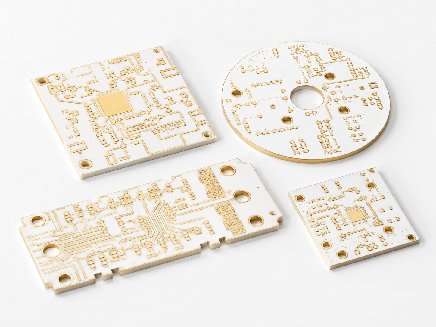
The ceramic PCB manufacturing process is the sequence of material preparation, substrate processing, circuit formation, metallization, finishing, inspection, and packaging used to produce ceramic-based printed circuit boards. Unlike standard FR4 boards, ceramic PCBs use inorganic ceramic substrates such as alumina, aluminum nitride, silicon nitride, or zirconia-toughened alumina.
The ceramic board itself is not only a carrier for copper circuits; it is also part of the thermal management structure. That is why the production route must be carefully controlled from raw ceramic substrate selection to final surface finish.
A typical ceramic PCB project may involve DPC, DBC, AMB, thick film, LTCC, or HTCC technology. Each process has its own material rules, conductor system, copper thickness range, and design restrictions. For example, DPC is often selected for fine circuits and high-density layouts, while DBC and AMB are widely used for higher-power applications that require thicker copper and stronger thermal paths.
EBest Circuit (Best Technology) supports ceramic PCB manufacturing and ceramic PCB assembly, with process capabilities covering materials such as Al2O3, AlN, ZTA, and Si3N4, as well as DPC, DBC, AMB, thick film, LTCC, and HTCC technologies. The company information also lists quality certifications including IATF 16949, ISO 9001:2015, ISO 13485:2016, AS9100D, REACH, RoHS, and UL.
What Ceramic PCB Materials Are Commonly Used?
Ceramic PCB materials are selected according to thermal conductivity, dielectric performance, mechanical strength, coefficient of thermal expansion, cost target, and end-use environment.
The most widely used ceramic PCB materials include alumina, aluminum nitride, silicon nitride, and zirconia-toughened alumina. Each material has a different engineering personality. Alumina is cost-effective and widely available. Aluminum nitride offers much higher thermal conductivity. Silicon nitride is valued for strength and thermal shock resistance. ZTA provides improved toughness compared with standard alumina.
| Ceramic PCB Material | Main Strength | Typical Use Case | Practical Selection Note |
|---|---|---|---|
| Alumina PCB, Al2O3 | Good insulation, stable performance, balanced cost | LED modules, sensors, power electronics, general ceramic circuits | A common starting point for ceramic PCB prototype and volume production |
| Aluminum Nitride PCB, AlN | High thermal conductivity, low thermal expansion | High-power LED, laser diode, RF power, power semiconductor modules | Chosen when heat dissipation is a leading design requirement |
| Silicon Nitride PCB, Si3N4 | High mechanical strength, thermal shock resistance | Automotive power modules, harsh-environment electronics | Suitable for applications with mechanical and thermal stress |
| ZTA Ceramic PCB | Better toughness than pure alumina | Industrial electronics, power control, demanding substrates | Useful when designers need stronger mechanical durability |
| LTCC Ceramic | Multilayer ceramic structure, embedded conductors | RF modules, filters, compact electronic packages | Suitable for compact multilayer ceramic circuits |
| HTCC Ceramic | High-temperature co-fired ceramic structure | Aerospace, high-temperature sensors, hermetic packages | Often selected for high-temperature and high-reliability environments |
Alumina is often the first choice when the design needs ceramic benefits at a reasonable cost. It offers good dielectric strength, chemical resistance, and mechanical stability. For many industrial and LED applications, alumina gives a practical balance between performance and budget.
Aluminum nitride is selected when thermal performance becomes more important. It transfers heat far more efficiently than alumina, which makes it attractive for high-power chips, laser components, high-brightness LED modules, and compact power devices. Its coefficient of thermal expansion is also closer to silicon, which can support better reliability in semiconductor-related designs.
Silicon nitride and ZTA are used when strength and fracture resistance become part of the design conversation. These materials are helpful in applications exposed to vibration, thermal cycling, or mechanical pressure. Although they may carry a higher cost, they provide valuable stability in demanding environments.
How Does the Ceramic Manufacturing Process Start?
For ceramic PCBs, the early stage usually includes engineering review and process selection. The supplier checks whether the design is better suited for DPC, DBC, AMB, thick film, LTCC, or HTCC. This decision has a direct influence on copper thickness, minimum line width, hole processing, surface finish, cost, and delivery time.
The beginning stage often includes:
- Reviewing Gerber files, drill files, drawings, stack-up, and copper thickness requirements.
- Confirming ceramic substrate type, such as alumina, AlN, Si3N4, or ZTA.
- Checking whether the circuit needs fine traces, thick copper, high-voltage spacing, or strong thermal transfer.
- Evaluating hole size, edge tolerance, board thickness, and panelization method.
- Confirming the surface finish for soldering, wire bonding, or long-term storage.
This early review is highly valuable for ceramic PCB prototype projects. Many prototypes are built for electrical testing, thermal testing, or mechanical validation. The ceramic production process also begins with substrate procurement or in-house substrate preparation. For standard alumina or aluminum nitride thicknesses, manufacturers may use pre-sintered ceramic sheets.
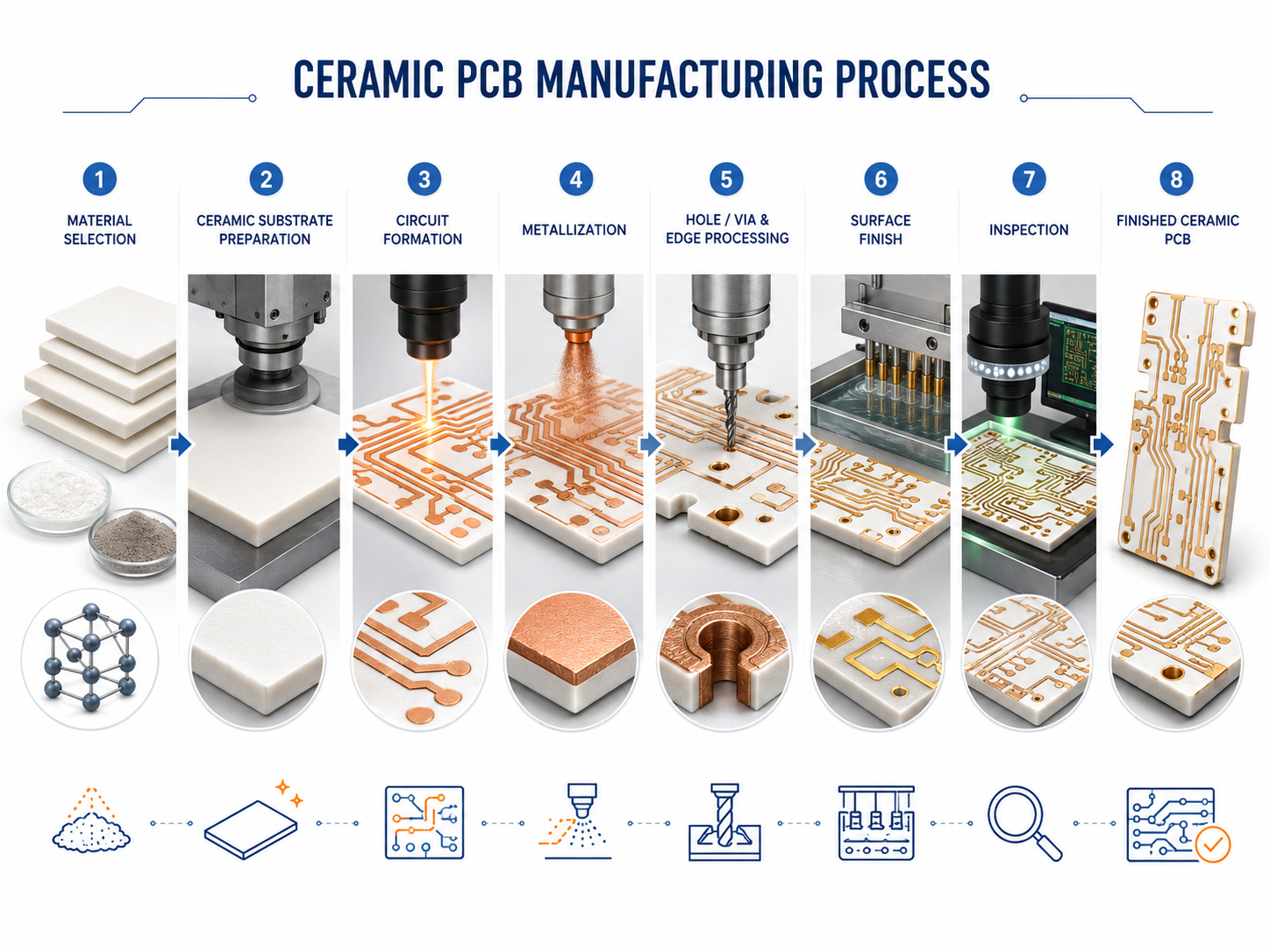
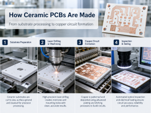
How Are Ceramic Substrates Prepared?
Ceramic substrate preparation creates the foundation for the entire board. A stable substrate supports accurate circuit formation, reliable metallization, clean edge processing, and strong assembly results. Any issue in flatness, thickness, surface quality, or internal structure can influence later steps.
In a traditional ceramic production process, ceramic powder is mixed with binders, solvents, plasticizers, and other additives. The mixture is shaped by tape casting, dry pressing, extrusion, or injection molding, depending on the substrate type and final application. After forming, the green ceramic body is dried and sintered at high temperature. During sintering, organic materials burn out and ceramic particles bond together into a dense, hard substrate.
For ceramic PCB manufacturing, many projects start from fired ceramic substrates. These sheets are inspected for thickness, surface condition, warpage, cracks, chips, and contamination. The substrate may then be cleaned, lapped, polished, laser-cut, drilled, or prepared for metallization.
Typical ceramic substrate preparation steps include cleaning, dimensional inspection, surface activation, laser drilling, contour pre-processing, and panel arrangement. Cleanliness is especially important because ceramic surfaces must bond well with copper, tungsten, silver, gold, or other metallization systems. Dust, oil, or weak surface energy can affect adhesion and long-term stability.
EBest Circuit’s ceramic PCB capability information includes common substrate thicknesses such as 0.38 mm, 0.635 mm, and 1.0 mm for Al2O3 and AlN, as well as 0.25 mm and 0.32 mm for Si3N4.
How Are Circuits Formed on Ceramic PCBs?
Circuit formation on ceramic PCBs depends on the selected manufacturing technology. The circuit can be built through direct copper plating, bonded copper foil, active metal brazing, thick film printing, or co-fired ceramic processing. Each route produces a different structure and supports different applications.
In DPC, or Direct Plated Copper, the ceramic surface is usually activated and plated with copper. This method supports fine circuits, good dimensional accuracy, and relatively thin copper layers compared with DBC or AMB. DPC is often chosen for LED substrates, sensors, optoelectronics, and ceramic PCB prototype work where precision is important.
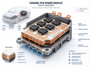
In DBC, or Direct Bonded Copper, copper foil is bonded directly to the ceramic substrate through a high-temperature bonding process. DBC ceramic PCBs can carry higher current and dissipate heat well, which makes them popular in power electronics, IGBT modules, automotive power systems, and high-power LED modules.
AMB, or Active Metal Brazing, uses active brazing materials to bond copper to ceramic. It is often used with silicon nitride ceramic because the bond strength and mechanical reliability are well suited for demanding power modules. AMB substrates can provide excellent thermal cycling performance and strong copper adhesion.
Thick film ceramic PCBs use screen printing to apply conductive paste onto the ceramic substrate. The printed circuit is then dried and fired. Conductive materials may include silver, palladium silver, gold, or other paste systems. Thick film technology is useful for hybrid circuits, sensors, heaters, resistive networks, and certain compact electronic modules.
LTCC and HTCC use co-fired ceramic technology. Conductive patterns are formed on ceramic green tapes, then stacked, laminated, and fired together. LTCC is often used for RF modules and compact multilayer circuits. HTCC is used for high-temperature and high-reliability packages.
| Circuit Formation Method | Brief Description | Suitable Applications | Main Advantage |
|---|---|---|---|
| DPC | Copper is plated onto ceramic after surface activation | Fine circuits, LED, sensors, prototypes | Good precision and clean circuit definition |
| DBC | Copper foil is bonded directly to ceramic | Power modules, high-current boards | Thick copper and strong heat transfer |
| AMB | Copper is brazed to ceramic with active metal | Automotive power, Si3N4 substrates | Strong bonding and thermal cycling reliability |
| Thick Film | Conductive paste is printed and fired | Hybrid circuits, sensors, heaters | Flexible patterning and mature process |
| LTCC | Ceramic tapes and conductors are co-fired | RF modules, compact multilayer designs | Multilayer integration |
| HTCC | High-temperature co-fired ceramic structure | Hermetic packages, aerospace, sensors | High-temperature endurance |
What Is the Role of Metallization in Ceramic PCB Manufacturing?
Metallization is one of the most important steps in ceramic PCB manufacturing because ceramic itself is insulating. To create electrical circuits, solderable pads, vias, and bonding areas, the ceramic surface must receive a conductive metal layer. This metal layer must bond firmly to the ceramic and remain stable during thermal cycling, soldering, and long-term operation.
The metallization system depends on the process type. DPC commonly uses sputtering or seed-layer deposition followed by copper electroplating. Thick film ceramic PCBs use fired metal pastes. LTCC and HTCC may use tungsten, molybdenum, silver, gold, or other conductor systems that can withstand the firing environment. DBC and AMB rely on copper bonding technology to create strong metal-ceramic adhesion.
In real production, metallization is controlled through surface preparation, metal thickness, adhesion testing, pattern accuracy, and inspection. For high-power boards, copper thickness becomes especially important. EBest Circuit’s ceramic PCB process information lists outer copper capability for DPC and thicker copper ranges for DBC and AMB, which reflects the different roles these processes play in precision circuits and power substrates.
Metallization also affects assembly choices. If the customer plans to use soldering, ENIG, immersion silver, immersion tin, or other solderable finishes may be selected. If the customer plans to use wire bonding, gold-related finishes may be more suitable. If the board will operate in a high-temperature or high-current environment, the metallization structure must be reviewed carefully during DFM.
How Are Holes, Vias, and Edges Processed?
Holes, vias, and edges are processed through laser machining, mechanical drilling, grinding, routing, dicing, or precision cutting. Ceramic is harder and more brittle than FR4, so these operations require controlled tooling and stable process parameters.
For ceramic PCBs, holes may be plated through holes, non-plated holes, laser vias, mounting holes, or thermal vias. The hole design depends on the circuit requirement and mechanical assembly method. Small holes are often made by laser drilling because ceramic material is difficult to machine with standard PCB drilling tools. Larger holes and edges may use CNC grinding, laser cutting, waterjet cutting, or diamond tooling.
Edge processing is also important. Ceramic boards often have tight outline tolerances, especially when used in power modules, LED packages, sensors, or custom housings. Chips, microcracks, and rough edges should be controlled because they may influence mechanical strength and assembly fit.
Typical hole and edge processing considerations include:
- Minimum plated and non-plated hole size.
- Hole tolerance and position accuracy.
- Aspect ratio for plated holes.
- Distance from circuit to board edge.
- Outline tolerance for custom shapes.
- Edge smoothness and chipping control.
- Panel format for production and assembly.
What Surface Finishes Are Used for Ceramic PCBs?
Surface finish protects exposed metal and supports soldering, wire bonding, storage, and assembly. Since ceramic PCBs are often used in high-reliability applications, the finish should match the component type, assembly method, bonding process, and operating environment.
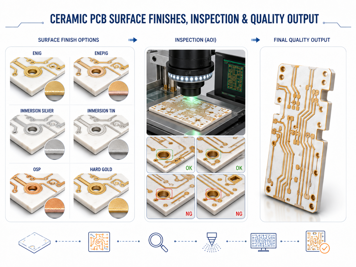
Common ceramic PCB surface finishes include ENIG, ENEPIG, immersion silver, immersion tin, OSP, hard gold, and sometimes special gold systems for wire bonding. The best option depends on whether the customer needs solderability, aluminum wire bonding, gold wire bonding, high wear resistance, or stable shelf life.
| Surface Finish | Brief Description | Suitable Use | Practical Note |
|---|---|---|---|
| ENIG | Nickel layer with thin immersion gold | SMT assembly, general soldering, stable storage | Popular and versatile for many ceramic PCB assemblies |
| ENEPIG | Nickel, palladium, and gold finish | Wire bonding and soldering | Good for advanced packaging and mixed assembly needs |
| Immersion Silver | Thin silver finish over copper | High-speed signals, soldering | Good conductivity and solderability with proper storage |
| Immersion Tin | Tin finish over copper | Soldering applications | Cost-friendly for selected designs |
| OSP | Organic protective coating | Shorter storage cycles and soldering | Simple finish for certain copper surfaces |
| Hard Gold | Electroplated nickel-gold finish | Wear areas, contacts, selected bonding pads | Useful where contact durability is important |
ENIG is often chosen because it gives good solderability and a flat pad surface. It is suitable for many ceramic PCB assembly projects. ENEPIG is selected when the board requires both soldering and wire bonding, especially in more advanced electronic packages. Hard gold may be used where repeated contact or wear resistance is required.
Surface finish thickness should be controlled. For example, nickel and gold thickness have a direct effect on soldering behavior and bondability. According to the supplied EBest Circuit capability data, available finishes include OSP, ENIG, immersion silver, immersion tin, ENEPIG, and hard gold, with listed thickness ranges for each finish.
What Factors Affect Ceramic PCB Cost?
Ceramic PCB cost is affected by material type, substrate thickness, copper thickness, process route, circuit density, hole structure, tolerance, surface finish, quantity, and assembly requirements.
The biggest cost factor is often the ceramic material itself. Alumina is usually more economical, while aluminum nitride and silicon nitride are more expensive because they offer stronger thermal or mechanical performance. The second major factor is the manufacturing process. DPC, DBC, AMB, thick film, LTCC, and HTCC do not share the same cost structure.
Copper thickness also matters. Thin copper for fine circuits is different from thick copper for power modules. DBC and AMB substrates with heavy copper require more material and tighter process control. Small holes, tight tolerances, complex outlines, and special surface finishes also increase production effort.
| Cost Factor | Why It Matters | Cost Impact |
|---|---|---|
| Ceramic material | Al2O3, AlN, Si3N4, and ZTA have different raw material costs | High |
| Manufacturing process | DPC, DBC, AMB, thick film, LTCC, and HTCC use different equipment and steps | High |
| Copper thickness | Thicker copper supports current and heat but needs more processing control | Medium to High |
| Board size and panel use | Larger or irregular boards may reduce panel efficiency | Medium |
| Hole and via design | Small holes, dense vias, and tight tolerances increase machining time | Medium |
| Surface finish | ENEPIG and hard gold cost more than simpler finishes | Medium |
| Quantity | Prototype orders carry more setup cost per piece | Medium |
| Testing and inspection | High-reliability applications may require more documentation and checks | Medium |
A good way to manage cost is to align the design with the real performance target. For example, if alumina meets the thermal requirement, there may be no need to choose aluminum nitride. If DPC provides enough copper thickness and line accuracy, DBC may not be necessary. If ENIG is enough for soldering, ENEPIG may only be needed when wire bonding is required. This kind of DFM thinking helps customers receive a board that performs well without unnecessary specification inflation.
FAQs About Ceramic PCB Manufacturing Process
- 1. What is the difference between ceramic manufacturing process and ceramic PCB manufacturing process?
| Item | Ceramic Manufacturing Process | Ceramic PCB Manufacturing Process |
|---|---|---|
| Main Goal | Make ceramic material or ceramic parts | Make an electronic circuit board on ceramic |
| Key Steps | Forming, drying, sintering, polishing | Substrate prep, metallization, circuit formation, finish, testing |
| Output | Ceramic plate, block, tube, or part | Ceramic printed circuit board |
| Main Focus | Material density, shape, strength | Electrical path, heat transfer, solderability, reliability |
| Typical Users | Ceramic parts buyers, industrial part makers | Electronics engineers, EMS companies, power module designers |
- 2. What is the difference between alumina and aluminum nitride ceramic PCB materials?
Alumina and aluminum nitride are both popular ceramic PCB materials, but they serve different performance levels. Alumina is widely used because it is stable, insulating, cost-effective, and available in many specifications. It is a strong choice for general ceramic PCBs, LED boards, sensors, and industrial circuits.
Aluminum nitride has much higher thermal conductivity. It is selected when heat must move away from chips or power devices quickly. This makes AlN a strong fit for high-power LED modules, laser diodes, RF power devices, semiconductor packaging, and compact power electronics.
- 3. Can ceramic PCB prototypes be made in small quantities?
Yes, ceramic PCB prototypes can be made in small quantities. Prototype production is common for thermal testing, electrical validation, LED module evaluation, power device testing, and new product development.
- 4. Are ceramic PCBs suitable for high-power electronics?
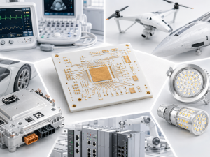
Yes, ceramic PCBs are highly suitable for high-power electronics. Their strong thermal conductivity, high insulation strength, and dimensional stability make them a preferred choice for power modules, LED lighting, automotive power systems, RF power devices, laser modules, and energy-related electronics.
- 5. What files does a ceramic PCB manufacturer need?
A ceramic PCB manufacturer usually needs complete production files and clear technical requirements. The more complete the documentation is, the smoother the review and quotation process will be.
Commonly requested files include:
- Gerber files for circuit layers, solder mask, silkscreen, and paste layers.
- Drill files for plated and non-plated holes.
- Mechanical drawing with board outline, thickness, tolerance, and special notes.
- Stack-up or substrate requirement, including ceramic material and thickness.
- Copper thickness requirement and surface finish selection.
- BOM and assembly drawing if ceramic PCB assembly is required.
- Special test requirements, such as electrical test, thermal inspection, or visual criteria.
- 6. How long does ceramic PCB production usually take?
Ceramic PCB production time depends on material availability, process type, quantity, complexity, surface finish, and whether assembly is included. A simple alumina DPC prototype may move faster than a customized AMB or LTCC project. Boards with special thickness, tight tolerances, heavy copper, or advanced finishes usually need more production planning.
- 7. Why are ceramic PCBs more expensive than FR4 PCBs?
Ceramic PCBs are more expensive than FR4 PCBs because the materials, equipment, and process controls are more specialized. FR4 is easy to laminate, drill, route, and process in large volumes. Ceramic substrates are harder, more brittle, and more demanding during drilling, cutting, metallization, and finishing.
In brief, the ceramic PCB manufacturing process turns a high-performance ceramic substrate into a reliable electronic interconnect through careful material selection, substrate preparation, circuit formation, metallization, machining, finishing, and inspection. For engineers working on power, LED, RF, medical, automotive, or industrial electronics, choosing the right ceramic PCB materials and an experienced ceramic PCB manufacturer can make product development smoother and more predictable. For ceramic PCB manufacturing, ceramic PCB prototype, or ceramic PCB assembly support, you can contact sales@bestpcbs.com
You may also like


Tags: ceramic manufacturing process, Ceramic PCB manufacturer, ceramic PCB materials, Ceramic PCB Prototype, ceramic production process