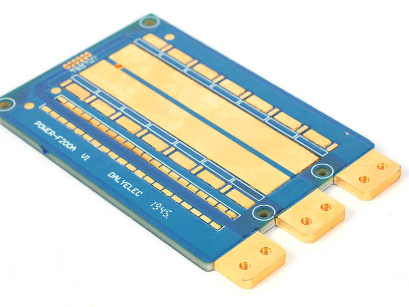
When engineers design high-current or high-heat boards, one wrong dimension can affect reliability. For embedded copper busbar PCBs, precision is everything. The copper block must fit perfectly within the PCB structure, the resin must flow correctly, and each layer must bond without gaps or warpage.
This part of our series focuses on the critical design parameters that determine performance and manufacturability. If you’re working on EV systems, solar inverters, or industrial power units, these details will help you design a board that balances strength, heat control, and electrical efficiency.
At EBest Circuit (Best Technology), we handle embedded copper busbar PCBs every day, from prototype to full production. Through that experience, we’ve learned exactly which parameters make or break a design.
Copper Thickness — The Foundation of Current Capacity
The copper thickness directly affects how much current your PCB can handle. In embedded copper designs, the copper block is not a thin foil; it’s a solid piece that typically ranges from 0.5mm to 3.5mm.
Common Thickness Options:
0.5mm, 0.6mm, 0.8mm, 1.0mm, 1.2mm, 1.6mm, 2.0mm, 2.5mm, 3.0mm, and 3.5mm
As a general rule:
- Thicker copper = lower resistance and higher current flow.
- However, it also requires tighter process control during lamination and drilling.
To maintain structural balance, the copper block should align with the overall board thickness. If the copper is too thick compared to the surrounding core layers, it can create stress points during press lamination, causing minor surface warpage or resin overflow.
At EBest Circuit (Best Technology), every design is reviewed through a copper-to-core ratio analysis before fabrication to avoid these issues.
Embedded Copper Thickness vs. Slot Depth
Getting the slot depth right is one of the most important design details. The slot is the cavity milled in the PCB core where the copper block will be placed.
Here’s a simplified guideline:
| Copper Thickness (mm) | Slot Depth Relation (PP + Core) |
| 0.5–0.6 | Equal to PP + Core slot depth |
| 0.8 | Copper block should be 0–0.05mm thicker |
| ≥1.0 | Copper block should be 0.05–0.1mm thicker |
This slight height difference ensures the copper surface aligns or slightly protrudes after lamination, maintaining direct contact for better thermal transfer.
If the copper block is too thin, resin may overfill the cavity, creating uneven surfaces. Too thick, and the board may warp or cause delamination during lamination.
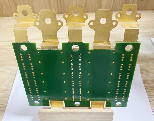
Minimum Copper Block Size
The size of the copper block determines whether the slot can be machined accurately and whether the resin can fill properly during lamination.
- Standard size: ≥3 × 3mm
- Minimum limit: 2.5 × 2.5mm
When blocks are smaller than 5 × 5mm, wire cutting is preferred over CNC milling. Wire cutting provides better accuracy and smoother edges, though it requires more time and cost.
For projects with more than 50 copper blocks per panel, wire cutting is again recommended to maintain dimensional consistency. At EBest Circuit (Best Technology), we maintain a tolerance of ±0.075mm to ensure perfect fit between the copper and slot.
Embedded Busbar PCB Copper Distance Rules
Spacing between copper blocks, drill holes, and traces is not just about meeting IPC standards — it’s about preventing delamination, short circuits, and stress concentration during drilling and operation.
Key Design Distances:
- Copper Block to Hole: ≥1.0mm (limit 0.8mm)
- Copper Block to Different-Net Copper: ≥0.5mm (limit 0.3mm)
By maintaining these distances, you help the board withstand thermal shock and mechanical vibration. In power systems that run at high current, this margin of safety is crucial for long-term stability.
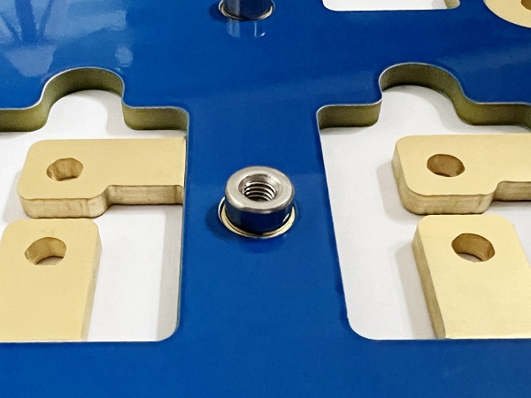
Slot Size and Tolerance
For best results, the slot in the PCB core and PP should be slightly larger than the copper block itself — typically 0.05mm clearance per side.
This minor difference allows the resin to flow evenly around the copper during lamination. If the fit is too tight, the resin may not fully penetrate, leading to small voids or weak bonding.
Corner design is also important. Both the copper block and slot corners should have a radius (R) of 0.8mm to reduce stress buildup and improve resin flow. Sharp corners are more likely to trap air or create cracks during curing.
Height Difference After Lamination
After lamination, the embedded copper should sit flush or slightly raised compared to the board surface. Standard height difference: 0 to +0.075mm
This ensures a smooth surface for solder mask and assembly, while still maintaining direct thermal contact. A copper block that sits too low could form an insulating resin layer that traps heat.
To guarantee uniform height, the lamination stack must be carefully balanced with high-resin PP materials.
Material Compatibility and PP Selection
The prepreg (PP) and core material play a vital role in lamination quality. Because embedded copper blocks have almost zero flexibility, the surrounding resin must be soft enough to fill gaps but strong enough to hold structure after curing.
Recommended PP Combination:
- Two layers of high-resin 1080PP
- Optional mixes: 106, 3313, 2116, or 7628
Important Notes:
- Always use at least two PP sheets between layers.
- Avoid PTFE materials — too soft for polishing and pressing.
- Rogers 4450F PP cannot be used (low flow and poor adhesion).
- For special laminates (TU-872SLK, M6, SH260, FR-27, FR-28), non-standard validation is required.
For special laminates (TU-872SLK, M6, SH260, FR-27, FR-28), non-standard validation is required.
Drilling Design and Hole Rules
Drilling through embedded copper requires separate parameters compared to FR-4 areas. The drill bit size must match copper hardness and thickness to avoid burrs and breakout.
| Red Copper Thickness (mm) | Minimum Drill Bit (mm) |
| 0.2–0.5 | ≥0.35 |
| 0.6–0.8 | ≥0.45 |
| 0.9–1.1 | ≥0.65 |
| 1.2–1.6 | ≥0.8 |
| 1.7–2.0 | ≥1.2 |
| 2.0–2.5 | ≥1.5 |
| 2.6–3.0 | ≥1.8 |
When drilling on copper areas, it’s best to process them separately from FR-4 zones. The Songlin machine handles copper hole drilling, while Dongtai or mass-production machines handle FR-4.
Inspection Standards to Validate the Design
Every embedded copper PCB should be inspected for dimensional accuracy and surface quality. Below are EBest Circuit (Best Technology)’s typical criteria:
- Height difference: +0.00mm to +0.075mm
- Dielectric strength: ≥ DC 1500V
- Thermal shock resistance: 288°C × 10s × 5 cycles, no delamination
- Plated copper thickness: ≥ 25μm
- Visual: No resin overflow, burrs, or oxidation around copper edges
These standards guarantee a stable electrical connection and strong mechanical bond, even under repeated thermal cycling.
Why Work with EBest Circuit (Best Technology)?
Designing embedded copper busbar PCBs requires both precision and experience. At EBest Circuit (Best Technology), we combine engineering support with real-world production knowledge to help customers achieve functional and cost-effective solutions. Here’s why customers choose us:
- Advanced equipment for wire cutting, depth-controlled milling, and core-to-core lamination.
- In-house DFM analysis for every embedded copper design.
- Compliance with IPC-6012 and IPC-600 standards.
- Dedicated engineering review to check stack-up balance, resin flow, and drill data before production.
When you need a manufacturer who truly understands busbar PCB design, our team will help you optimize every detail. EBest Circuit (Best Technology) is here to assist with every stage — from DFM validation to final testing — so your next high-power PCB design performs exactly as intended.