

As electronic products become smaller and more complex, engineers rely on different types of vias in PCB layouts to achieve dense routing, high-speed signal integrity, and thermal stability. Without vias, multilayer PCB architecture would not function efficiently. Each via structure serves a specific purpose. Some focus on basic connectivity, others support HDI routing, RF performance, or thermal transfer.
A typical multilayer PCB may contain hundreds or even thousands of vias depending on circuit density. According to common PCB fabrication guidelines, the most frequently used via diameter ranges between 0.2 mm and 0.5 mm, while high-density designs may use microvias smaller than 0.15 mm.
In this guide, we explain the most widely used PCB via types, how they work, and when engineers should apply them. The article also compares via filling technologies and explains the difference between vias and PTH holes.

1. Through-Hole Vias
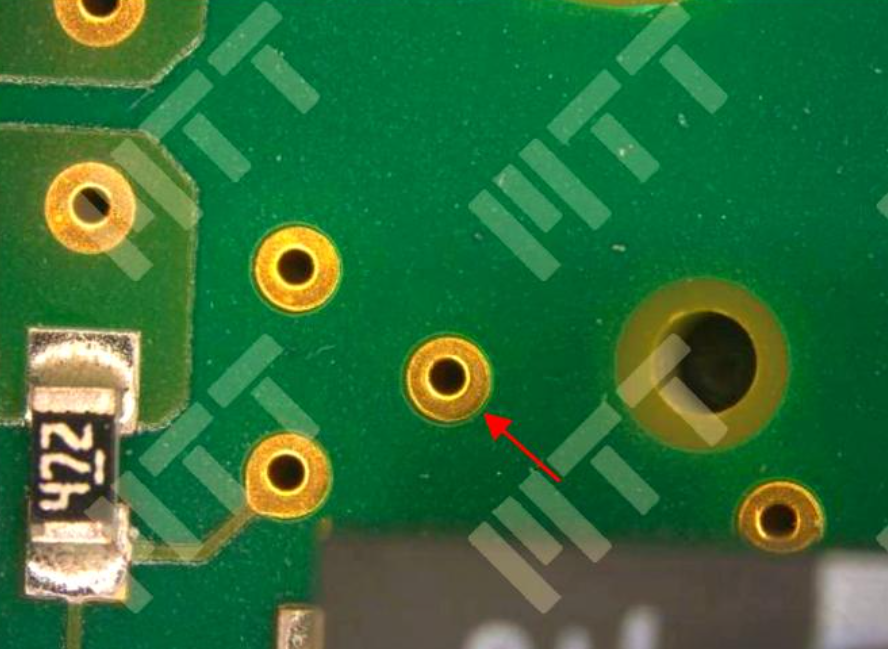
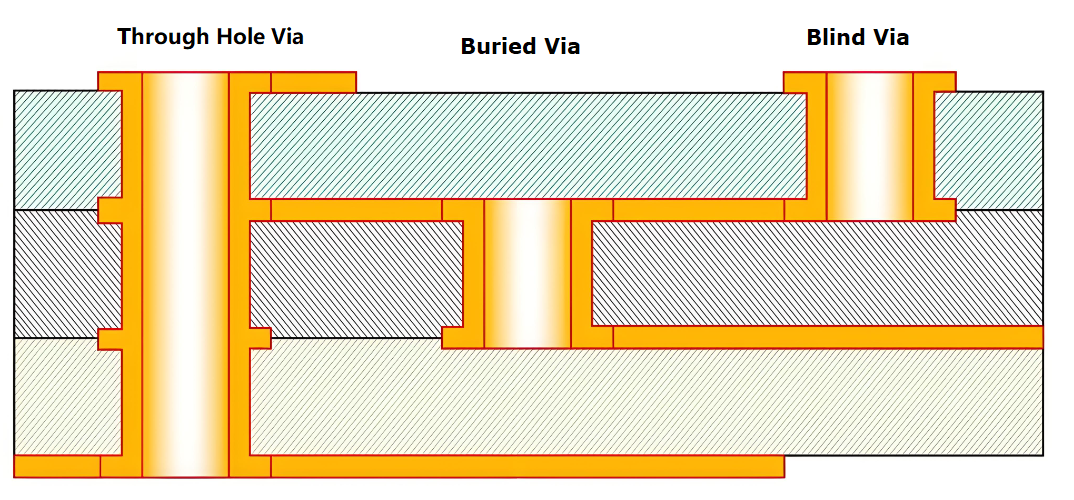
Through-hole vias are the most traditional and widely used PCB via types. They pass completely through the entire PCB stack, connecting the top layer to the bottom layer. In standard PCB manufacturing, mechanical drilling machines can achieve drill diameters from 0.15 mm to 6 mm. For most multilayer boards, the common finished via hole size ranges from 0.2 mm to 0.4 mm.
Another important parameter is the aspect ratio, which describes the ratio of board thickness to via hole diameter. Most PCB manufacturers recommend keeping the aspect ratio within 6:1 to 10:1 to ensure stable plating quality.
Typical characteristics of through-hole vias:
- Connect all PCB layers
- Larger drill diameters compared with HDI vias
- Lower fabrication cost
- Suitable for conventional multilayer PCB designs
- Reliable mechanical strength
However, through-hole vias occupy routing space on every layer they pass through. This can reduce layout flexibility when board density increases.
Typical applications include:
- Power distribution networks
- Ground connections
- Standard digital circuits
- Industrial electronics
Despite newer HDI technologies, through-hole vias remain an essential structure in many PCB designs.
2. Blind Vias
Blind vias connect the outer layer of a PCB to one or more inner layers, but they do not extend through the entire board.
For example, a blind via may connect the top layer to layer two or layer three, while leaving the remaining layers untouched. This design helps engineers save routing space on deeper layers.
Typical blind via depths are usually less than 0.3 mm, depending on the PCB stack-up structure. Laser-drilled blind vias often have diameters between 0.075 mm and 0.15 mm.
Advantages of blind vias include:
- Improved routing density
- More available space on internal layers
- Better signal routing for compact boards
- Reduced interference between layers
Blind vias are widely used in high-density electronics where layout space is limited.
Common applications include:
- Smartphones
- IoT devices
- compact industrial controllers
- RF modules
Blind vias help designers maintain a clean routing structure without drilling through the entire PCB stack.
3. Buried Vias
Buried vias connect inner PCB layers but do not reach the outer layers. They remain completely hidden within the board structure after lamination.
These vias are created during intermediate lamination stages. Manufacturers first drill and plate the internal layers, then laminate additional layers on top.
Typical buried via diameters are similar to standard mechanical vias, usually ranging from 0.2 mm to 0.3 mm.
Benefits of buried vias include:
- Increased routing density
- Cleaner surface layout
- Reduced via congestion
- Better signal performance in complex designs
However, buried vias increase fabrication complexity. They also require multiple lamination cycles.
For example, a PCB with buried vias and blind vias may require 2–3 lamination cycles, increasing production cost.
Typical uses include:
- HDI PCB designs
- advanced communication equipment
- networking hardware
- high-performance computing systems
Buried vias are especially useful when engineers must route many signals across multiple layers.
4. Stacked Vias
Stacked vias are a vertical arrangement of microvias placed directly on top of each other. Each microvia connects two adjacent layers, this structure creates a continuous vertical connection through several layers.
Stacked vias are commonly used in HDI PCB designs. They support extremely high routing density and are often placed under fine-pitch components such as BGA packages. Fine-pitch BGA packages often have ball pitches of 0.5 mm or smaller, making stacked microvias necessary for signal escape routing.
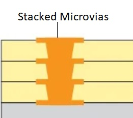
Key characteristics of stacked vias:
- Vertical alignment of multiple microvias
- Supports high-density routing
- Suitable for fine-pitch BGA packages
- Requires via filling and copper plating
Because stacked vias require precise alignment and filling processes, manufacturing cost is higher.
However, the structure provides excellent electrical performance and compact routing paths.
5. Staggered Vias
Staggered vias are an alternative to stacked vias. Instead of aligning microvias vertically, each via is slightly offset from the one above or below.
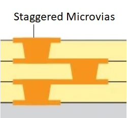
Advantages of staggered vias include:
- Improved mechanical reliability
- Lower fabrication difficulty
- Reduced risk of via cracking
- Suitable for HDI structures
Engineers often choose staggered vias when cost control is important but high routing density is still required.
These vias are frequently used in:
- consumer electronics
- automotive control boards
- communication equipment
Staggered vias provide a balanced solution between performance and manufacturing complexity.
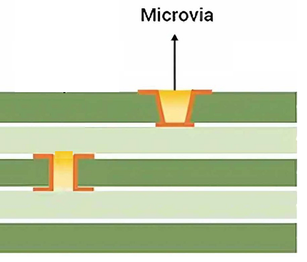
6. Microvias
Microvias are very small vias typically created by laser drilling. They are an essential element of HDI PCB technology. Microvias usually connect only two adjacent layers, so their diameter is significantly smaller than traditional vias. Typical microvia diameter ranges between 50 μm and 150 μm.
Because of their small size, microvias allow designers to route signals between fine-pitch component pads.
Key advantages of microvias:
- Extremely high routing density
- Shorter signal paths
- Lower parasitic inductance
- Improved signal integrity
Microvias are commonly used in advanced electronics such as:
- smartphones
- wearable devices
- aerospace systems
- high-speed communication equipment
Although microvias improve performance, they require specialized fabrication equipment and strict process control.
7. Vias in Pad
Vias in pad refer to vias placed directly inside the component pad area. This design is common in fine-pitch packages such as BGA or QFN devices. The via allows signals to transition immediately from the pad to inner routing layers.
However, vias in pad require filling and planarization before component assembly. Without proper filling, solder can flow into the via hole during reflow.
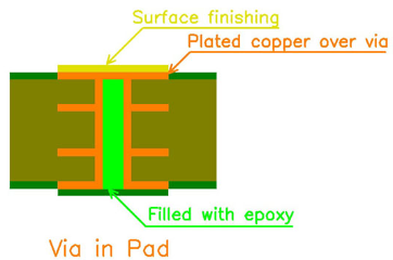
Advantages of vias in pad include:
- Reduced signal path length
- Improved routing density
- Better thermal transfer
- Ideal for fine-pitch BGA packages
8. Vias on Pad
Vias on pad are slightly different from vias in pad. In this structure, the via is placed very close to the pad rather than directly inside it.
The via may partially overlap with the pad area depending on design requirements. This method helps engineers maintain efficient routing while reducing the risk of solder wicking.
Key features of vias on pad include:
- Easier manufacturing compared with via-in-pad
- Lower cost than filled vias
- Suitable for many standard BGA layouts
- Good compromise between density and reliability
Designers often use this structure when full via-in-pad technology is not required.
What Is the Difference Between Via and PTH in PCB?
Many engineers confuse vias with plated through holes (PTH). Although they share a similar manufacturing process, their functions differ.
The following table explains the main differences.
| Feature | Via | PTH (Plated Through Hole) |
| Main function | Electrical interconnection between layers | Mounting hole for components |
| Diameter | 0.1–0.5 mm typical | 0.6–1.2 mm typical |
| Component insertion | Not intended for component leads | Designed for component leads |
| Assembly process | No component insertion | Used in through-hole assembly |
| Common use | Signal routing and power connections | Mechanical support and electrical connection |
In simple terms, a via connects PCB layers, while a PTH hole supports component leads while also providing electrical connectivity.
Via Filling Types in PCB
In advanced PCB manufacturing, vias are often filled to improve reliability and assembly quality. Several via filling methods are commonly used, including:
1. Conductive Paste Fill
Conductive paste fill involves filling the via with a conductive material such as silver epoxy.
Advantages:
- Good electrical conductivity
- Relatively simple process
- Suitable for certain thermal applications
However, paste materials may not provide the same mechanical strength as copper filling.
2. Resin Plugging
Resin plugging uses epoxy resin to fill the via hole. After filling, the surface is planarized to create a flat pad.
Key benefits include:
- Prevents solder wicking
- Improves assembly reliability
- Suitable for via-in-pad structures
Resin plugging is widely used in HDI PCBs and BGA assemblies.
3. Copper Fill (Via Plating)
Copper filling is the most advanced via filling method. The via hole is completely filled with electroplated copper.
Advantages include:
- Excellent thermal conductivity
- Strong mechanical stability
- High electrical reliability
- Ideal for stacked microvias
Copper-filled vias are common in high-performance PCBs used in aerospace, telecommunications, and advanced computing systems.
EBest Circuit: One-Stop PCB Manufacturer with Any PCB Via Types
At EBest Circuit (Best Technology), we support a wide range of PCB via structures for both standard multilayer boards and advanced HDI designs. Our engineering team works closely with customers during the early design stage to review via structures, optimize manufacturability, and improve long-term reliability.
Our capabilities include:
- Mechanical drilling down to 0.15 mm
- Laser microvia drilling to 75 μm
- HDI stack-up structures such as 1+N+1, 2+N+2, 3+N+3, 4+N+4
- Copper-filled stacked microvias
- Blind and buried via fabrication
- Professional DFM review before production
- Guidance on selecting the right PCB via types
- Optimization for HDI stack-up structures
- Manufacturing support for microvias, blind vias, and buried vias
- Full PCB fabrication and PCBA assembly service
If you are designing a multilayer PCB or HDI board and need professional manufacturing support, working with an experienced PCB partner can simplify the entire development process.
For project consultation, DFM review, or PCB manufacturing services, feel free to contact EBest Circuit (Best Technology) at: sales@bestpcbs.com. Our engineering team is always ready to help bring your PCB designs into reliable production.
Tags: different types of vias in pcb, pcb via types, types of vias in pcb, via types in pcb