

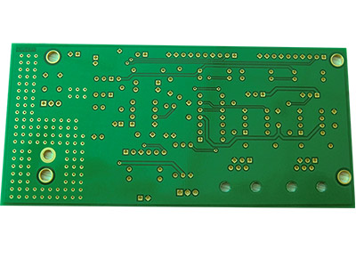
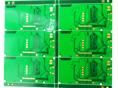
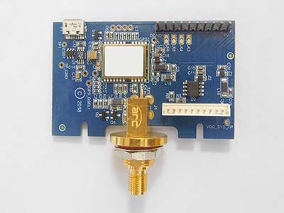
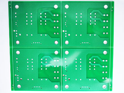
HDI PCB (High Density Interconnector PCB), is a printed circuit board having a relatively high line distribution density using the micro-blind and buried hole technology.
It is a process that includes an inner layer line and an outer layer line, then uses a hole and a metallization in the hole to realize a joint function between the inner layers of each layer.
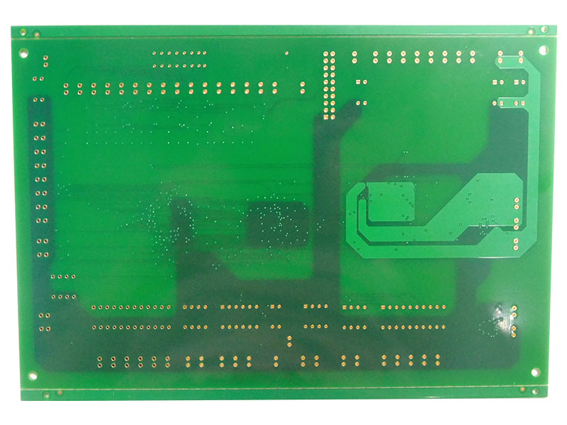
With the development of high-density, high-precision electronic products, the requirements of high-density and high precision are imposed on printed circuit boards. The most effective way to increase the density of pcb is to reduce the number of through holes, and to accurately set the blind holes and buried holes to achieve this requirement, thereby an HDI PCB came into being.
HDI PCBs are finding their way into a growing number of products:
Military communications devices and other strategic equipment
Aerospace – smaller space requirements and light weight are ideal for such applications
Computers and smartphones – phones and computers are taking full advantage of smaller profiles, reduced weight, and increased functionality, made possible through the integration of HDI circuits.
Medical equipment – diagnostic and monitoring equipment has become more reliable and expanded with technical features that aid medical teams with patient treatment, and all of this is powered by HDI PCBs and advanced software.
Benefits of HDI PCB
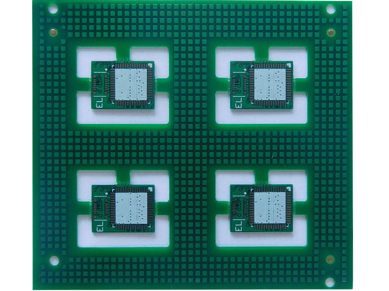
HDI PCB utilizes buried or blind vias, or a combination, and may also incorporate microvias with an incredibly small diameter. This facilitates the incorporation of more technology in less space, with fewer layers. Multi-layer HDI PCB are also in common use, with many layers being accommodated through various construction methods utilizing blind, buried, stacked, and staggered vias.
With smaller components and blind via in pad technology, components may be placed closer together, resulting in faster signal transmission rates while also reducing crossing delays and signal loss. These are key considerations that generate improved performance of HDI PCBs.
HDI PCBs are preferred for applications where space, performance, reliability, and weight are concerns. This makes them more suitable for nearly every application related to electronics, consumer products, computers, and aeronautics.
Multi-layer HDI PCB can provide strong interconnection of stacked vias, resulting in high levels of reliability, even in more extreme environments.
Considering this, do you ever think about choosing HDI PCB on your next project?
You may also like


Tags: HDI PCB