Copper base PCB delamination is one of the most frustrating and critical issues for engineers and buyers alike. When layers of the PCB separate, it compromises thermal performance, mechanical strengthen electrical safety. Whether it happens during soldering or while in use, understanding how to prevent and respond to delamination is vital for long-term reliability.
What Is Delamination in Copper Base PCBs?
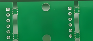
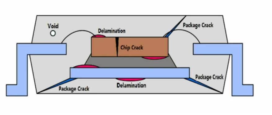
Delamination refers to the separation of different material layers in the copper base PCB structure. This usually occurs between the copper foil and the insulating dielectric or between the dielectric and the metal base. It is often visible as bubbles, warping, or peeling, and can even lead to electrical failure.
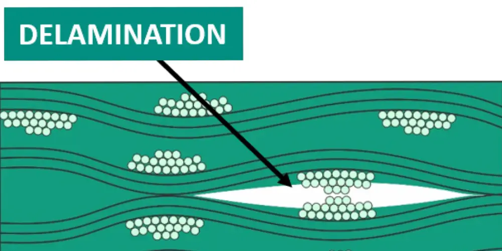
Delamination is a sign of poor adhesion, excessive internal stress, or improper material pairing. While it may seem like a production flaw, in many cases, it is a result of both design and process-related decisions.
Common Causes of Delamination in Copper Base PCB
1. Mismatch in Thermal Expansion Coefficient (CTE)
The CTE mismatch between copper, dielectric resin, and metal base can generate internal stress during temperature cycling, leading to separation over time.
2. Poor Lamination Process
If the lamination pressure is too low, or the vacuum environment is inadequate, resin will not bond well with copper. This creates weak interfaces that can easily delaminate during reflow or wave soldering.
3. Excessive Heat or Thermal Shock
Copper base PCBs used in LED, power, or automotive sectors often undergo extreme temperatures. Rapid heating or cooling during soldering can exceed the material’s limit and cause bubbling or blistering.
4. Moisture Absorption
If the PCB absorbs moisture during storage or processing, it will vaporize during soldering, forming vapor pressure that forces the layers apart.
5. Mechanical Drilling Stress
For thick copper or multilayer copper base PCBs, improper drilling parameters may introduce mechanical stress that fractures the resin bond.
Signs That Your Copper Base PCB Is Delaminating
- Bubbles or bulges under the copper foil
- Peeling or flaking of surface copper
- Warping or deformation after soldering
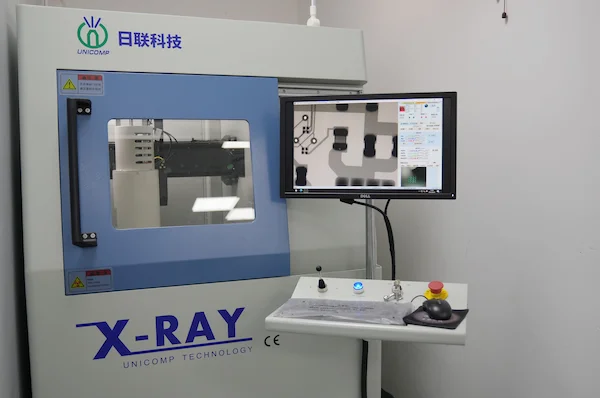
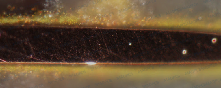
- Burn marks or internal voids seen in X-ray or ultrasonic scans
- Circuit opens or intermittent connections
How to Handle Delamination During Production?
If you detect delamination during prototype or volume production:
1. Stop and Identify the Root Cause:
- Perform cross-sectional analysis of the delaminated area.
- Check resin flow, press temperature, and bonding pressure during lamination.
- Verify vacuum level and lamination time.
2. Adjust the Lamination Process:
- Increase bonding pressure and resin flow time.
- Use vacuum lamination with temperature ramping.
- Switch to a resin system with better heat resistance and adhesion.
3. Dry the Material Before Lamination:
- Bake prepregs and metal cores at 120–150°C for 2–4 hours to eliminate moisture.
4. Use Better Dielectric Materials:
- Use thermally conductive epoxy with higher Tg and lower CTE.
- Consider ceramic-filled resins for high-power applications.
What If Delamination Happens After Delivery?
If the copper base PCB delaminates during customer assembly or field use:
1. Check if soldering parameters were too aggressive
Overheating or reflow profiles with steep ramps can cause internal separation.
2. Inspect PCB storage and packaging
Improper vacuum sealing or exposure to humidity can lead to moisture buildup.
3. Request reliability test reports from the supplier
Ensure your supplier provides thermal cycling, cross-section, and peel strength data for the batch.
How to Prevent Delamination in Copper Base PCB Designs?
Preventing delamination requires a combined effort in material selection, stack-up design, processing parameters, and storage control. Here’s how to prevent & reduce the risk of delamination from the ground up.
1. Use High-Quality Dielectric Materials
One of the most direct ways to prevent delamination is choosing a dielectric layer with excellent adhesion properties and low moisture absorption. In copper base PCB design, typical dielectrics include thermally conductive epoxy, ceramic-filled resin, or polyimide.
What to look for in dielectric material:
- High Tg (Glass Transition Temperature) above 150°C
- Low CTE (Coefficient of Thermal Expansion) for better mechanical stability
- High peel strength to enhance bonding with copper
- Thermal conductivity ≥ 1.0 W/m·K for effective heat transfer
2. Choose the Right Stack-up for Your Application
If your design needs high thermal conductivity, select a resin with high Tg and low CTE to reduce internal stress.
3. Design Even Copper Distribution
Avoid heavy copper areas on one side only, which can cause warping or asymmetrical expansion during soldering.
4. Pre-bake the PCB Before Reflow
Even if your supplier provides vacuum-packed boards, pre-baking before SMT helps prevent delamination from moisture.
5. Set Realistic Soldering Profiles
Avoid shock heating. Ramp temperature gradually and stay within resin limits.
6. Proper Drill Parameters and Hole Cleaning
For multilayer copper base PCBs, drilling through copper and resin layers generates mechanical stress. Improper drill speed, feed rate, or dull drill bits can cause micro-cracks, which may propagate and cause delamination.
7. Avoid Sharp Thermal Transitions in Reflow Soldering
Rapid heating or cooling causes materials to expand or contract at different rates. If the resin can’t keep up, it will delaminate.
Copper base PCB delamination is not just a fabrication problem — it’s also a design and process challenge. By carefully selecting materials, managing thermal profiles, and working with professional PCB manufacturers, you can significantly reduce the risk.
FAQs
Q1: What causes copper base PCB to delaminate after soldering?
Rapid heating, high peak temperature, or moisture buildup in the board are the most common causes.
Q2: How can I test whether my copper base PCB has internal delamination?
You can use ultrasonic scanning (C-SAM), X-ray imaging, or destructive cross-sectioning.
Q3: What’s the ideal copper thickness to reduce delamination risk?
While thicker copper helps heat dissipation, it also introduces stress. A balance between 2oz–4oz copper and suitable resin is ideal.
Q4: Can I rework a delaminated copper base PCB?
In most cases, no. Once delaminated, the structural and electrical integrity is compromised.
Q5: What files should I provide to the manufacturer to ensure better reliability?
Gerber files, stack-up drawing, copper weight details, thermal simulations (if any), and assembly temperature profiles.
Why Choose Best Technology?
Best Technology specializes in high-reliability copper base PCBs for LED, power, and automotive markets. We apply vacuum press lamination, use high-Tg resins, and perform 100% inspection on thermal integrity. Whether you need single-layer, double-layer, or heavy copper designs, we provide reliable solutions backed by engineering support.
Let us help you optimize your copper base PCB design to prevent delamination and maximize thermal and mechanical stability.