

PCB panelization is a critical step in the manufacturing process that directly impacts production efficiency, material waste, and overall costs. Poor panel design can lead to lower yields, increased scrap, and delays in assembly. In this blog, we’ll explore actionable strategies to optimize PCB panelization for higher yield and cost savings.
Why Panelization Matters in PCB Manufacturing?
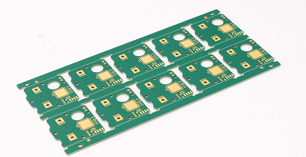
Panelization refers to arranging multiple PCB designs onto a single manufacturing panel (or “array”) for batch processing. Key benefits include:
- Reduced material waste: Maximizing panel space utilization.
- Faster assembly: Enabling automated pick-and-place machines to process multiple boards simultaneously.
- Lower handling costs: Fewer individual boards to manage during fabrication and assembly.
However, suboptimal panelization can lead to:
- Warpage during soldering.
- V-score or routing errors.
- Increased breakage during depaneling.
6 Tips to Optimize PCB Panelization
Base on our 19+years experiences in the PCB manufacturing field, today I would like to share you 6 Strategies to Optimize PCB Panelization
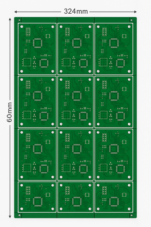
1. Choose the Right Panel Size
- Align your PCB dimensions with standard panel sizes (e.g., 18″x24″, 21″x24″) to minimize material trimming.
- Example: If your board is 80mm x 60mm, arrange 4×6 units on a 324mm x 480mm panel to reduce unused space.
2. Optimize Board Arrangement
- Rotation: Rotate boards to fit more units per panel.
- Mirroring: Use symmetrical designs to avoid “wasted” gaps.
- Nesting software: Leverage tools like CAM350 to automate optimal layout generation.
3. Select the Best Depaneling Method
The choice of depaneling (separating individual boards) affects yield and edge quality:
- V-Score: Low cost and fast, but requires straight edges and may weaken boards.
- Tab Routing: Ideal for irregular shapes but adds milling time.
- Laser Cutting: Precision for high-density designs, but higher cost.
Rule of thumb: Use V-score for rectangular boards and routing for complex shapes.
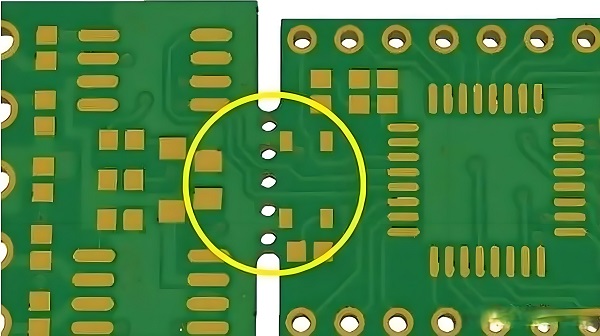
4. Add Breakaway Tabs and Mouse Bites
- Breakaway tabs: Small connectors between boards to prevent movement during assembly.
- Mouse bites: Perforated holes for easy manual separation.
- Spacing: Maintain 1.5–2mm between boards to avoid solder mask bridging.
5. Incorporate Fiducials and Tooling Holes
- Add global fiducials to the panel for accurate alignment during SMT assembly.
- Include tooling holes (3.2mm diameter) to secure the panel during drilling and routing.
6. Balance Quantity vs. Risk
- Overcrowding panels increases the risk of cross-board defects.
- Underutilizing panels raises material costs.
- Recommended: Aim for 4–20 boards per panel, depending on size and complexity.
Case Study: Cost Savings Through Smart Panelization
A consumer electronics manufacturer redesigned their 50mm x 50mm IoT module panel:
- Initial design: 8 boards/panel with 15% wasted space.
- Optimized design: 12 boards/panel using rotated layouts and shared tooling holes.
- Results:
- 15% reduction in material costs.
- 10% faster SMT assembly.
- Fewer depaneling errors due to improved tab routing.
Common Panelization Mistakes to Avoid
- Ignoring manufacturer capabilities: Always consult your PCB fab’s panel size and tolerances.
- Overcomplicating shapes: Complex panels increase milling time and scrap rates.
- Skipping test coupons: Include test patterns for impedance control and quality checks.
Conclusion
Optimizing PCB panelization requires a balance of geometric efficiency, process knowledge, and collaboration with manufacturers. By implementing these strategies, you can reduce waste, improve yields, and lower production costs without compromising quality.
Pro Tip: Use panelization-specific design rules in tools like Altium or KiCad to automate compliance checks.
Also, if you want to know more about how to optimize PCB Panelization for Higher Yield and Lower Cost, please feel free to inquiry from us.
You may also like


Tags: pcb panelization