





A diamond heat spreader can move concentrated heat away from a small, high-power device far faster than common metals. That advantage is attracting attention as AI accelerators, RF power amplifiers, GaN devices, laser diodes, and advanced power modules place more heat into less area. But a high material conductivity does not automatically produce a cooler junction.
Whether it helps depends on the complete thermal path: heat-source size, spreader thickness and area, thermal expansion, metallization, bond-line quality, downstream heat sink, and operating conditions. What matters is where the largest temperature drop occurs and how much of it the diamond layer can actually remove. That is what connects the material’s impressive conductivity with its real effect on junction temperature and cost.
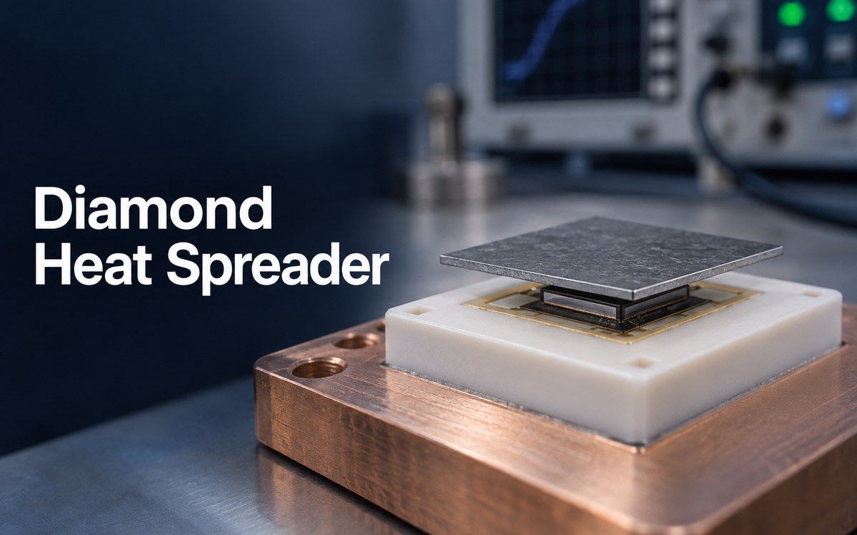
What Is a Diamond Heat Spreader?
A diamond heat spreader is a thin synthetic-diamond plate positioned close to a concentrated heat source. Its purpose is to distribute heat over a larger area before that heat enters a heat sink, cold plate, package lid, metal base, or other cooling structure.
Most electronic heat spreaders use chemical vapor deposition, or CVD, diamond. The manufacturing process grows diamond from a carbon-containing gas rather than cutting it from natural gemstone material. Different growth conditions and material grades produce different thermal conductivity, surface finish, thickness, and cost.
The spreader does not remove heat from the system by itself. It reduces the temperature gradient near the device and presents a larger effective area to the next part of the cooling path.
For example, a small GaN die may generate intense local heat. If it contacts a much larger copper plate directly, heat must spread laterally through copper near the die before the full plate area becomes useful. A diamond layer can distribute that heat more quickly, helping more of the downstream cooler participate.
This distinction matters because the following two statements are not equivalent:
- the spreader material has very high thermal conductivity;
- the assembled device has low junction-to-cooler thermal resistance.
The first describes a material property. The second depends on the diamond, its geometry, both attachment interfaces, the package, and the final cooling system.
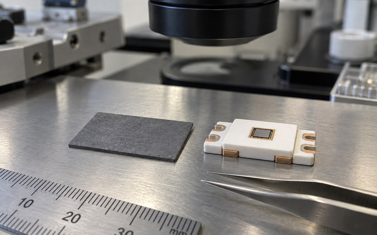
Diamond Thermal Conductivity vs Copper: Does the Material Number Tell the Whole Story?
No. Diamond can conduct heat several times better than bulk copper, but conductivity alone cannot predict the finished temperature.
High-quality CVD diamond is commonly available across a broad thermal-conductivity range, with premium grades reaching roughly 2,000 W/m·K or more. Bulk copper is commonly treated as approximately 400 W/m·K near room temperature. This makes diamond attractive when a small device produces a steep local temperature gradient.
For one-dimensional conduction, thermal resistance can be approximated as:
R = t / (k × A)
Where:
- R is thermal resistance;
- t is material thickness;
- k is thermal conductivity;
- A is the effective heat-transfer area.
The relationship shows why conductivity matters, but it also shows why a material number is not enough. A thicker layer increases through-thickness resistance. A larger contact area reduces it. Real heat flow is also three-dimensional, so lateral spreading and edge geometry affect the result.
The interfaces may be even more important. A thick solder layer, voided braze joint, uneven metallization, warped surface, or poorly compressed thermal interface can add enough resistance to hide much of the diamond advantage. If the external heat sink or cold plate is already the dominant bottleneck, replacing a copper spreader with diamond may produce only a small improvement.
Thermal expansion also changes the result. Diamond expands much less than copper as temperature changes. That can be helpful near some semiconductor materials, but the complete assembly must accommodate differences among the die, metallization, solder or braze, substrate, copper features, and housing. A design that performs well at room temperature may still develop stress during reflow, power cycling, or environmental testing.
The useful comparison is therefore not “diamond versus copper conductivity.” It is the predicted and measured junction temperature for two complete, manufacturable thermal stacks.
CVD Diamond Heat Spreader vs Copper-Diamond Heat Spreader: Which Structure Fits?
CVD diamond provides the highest potential for local heat spreading, together with electrical insulation and low mass. Copper-diamond composites combine improved conductivity with metal-like structural integration and more moderate thermal-expansion behavior.
| Comparison point | CVD diamond heat spreader | Copper-diamond heat spreader |
|---|---|---|
| Basic structure | Polycrystalline or single-crystal synthetic diamond | Diamond particles distributed through a copper matrix |
| Thermal performance | Highest potential conductivity, depending on grade | Typically higher than copper but below premium CVD diamond |
| Electrical behavior | Diamond itself is electrically insulating | Copper matrix is electrically conductive |
| Mechanical processing | Hard and difficult to machine; often laser cut | Usually more compatible with metal-style machining and larger structures |
| Interface preparation | Frequently needs controlled metallization for soldering, brazing, or die attach | May integrate more naturally with metal lids, bases, or cold-plate features |
| Typical use | Local hot-spot spreading close to a die or RF device | Package lids, inserts, carriers, bases, and larger heat-spreading structures |
| Common limitation | Interface resistance can prevent the assembly from using its premium conductivity | Performance varies with diamond content, particle distribution, porosity, and construction |
CVD diamond is not one fixed material. Black, opaque, translucent, and optical grades can have different purity and conductivity ranges. The highest-conductivity grade is not automatically the best fit for every assembly. A lower grade may reach the same temperature target when interface resistance or downstream cooling limits the benefit.
Copper-diamond is also not simply “copper plus diamond.” Diamond content, particle size, particle distribution, interface quality, porosity, copper alloy, and manufacturing route affect thermal conductivity and thermal expansion. The published material values are meaningful only when they correspond to the actual grade and test method.
The two structures therefore serve different physical roles. CVD diamond is better suited to a thin, electrically insulating layer close to an intense hot spot. Copper-diamond is better suited to a larger lid, insert, carrier, or machined structure that must spread heat while remaining part of a metal assembly.
Is a Diamond Heat Spreader the Same as a Diamond Heat Sink?
Not usually. A heat spreader distributes concentrated heat across a larger area. A heat sink transfers that heat into air, liquid, a chassis, or another external cooling medium.
A diamond plate placed directly under a die is normally a heat spreader. It reduces the local hot spot and moves heat toward a larger copper base, aluminum heat sink, vapor chamber, cold plate, or package lid. That larger structure then removes heat from the assembly.
The terms can overlap in supplier descriptions because a diamond part may perform both functions in a specialized device. However, calling every diamond plate a heat sink can hide an important engineering question: where does the heat go after it leaves the diamond?
A complete thermal path may include:
- semiconductor junction and die;
- die-attach or thermal bond layer;
- metallized diamond heat spreader;
- package carrier, ceramic substrate, MCPCB, or metal base;
- thermal interface material;
- heat sink, cold plate, enclosure, or chassis;
- air or liquid coolant.
Improving one element helps only if the remaining path can accept and remove the transferred heat. A diamond spreader connected to an undersized heat sink can distribute heat efficiently while the complete system still overheats.
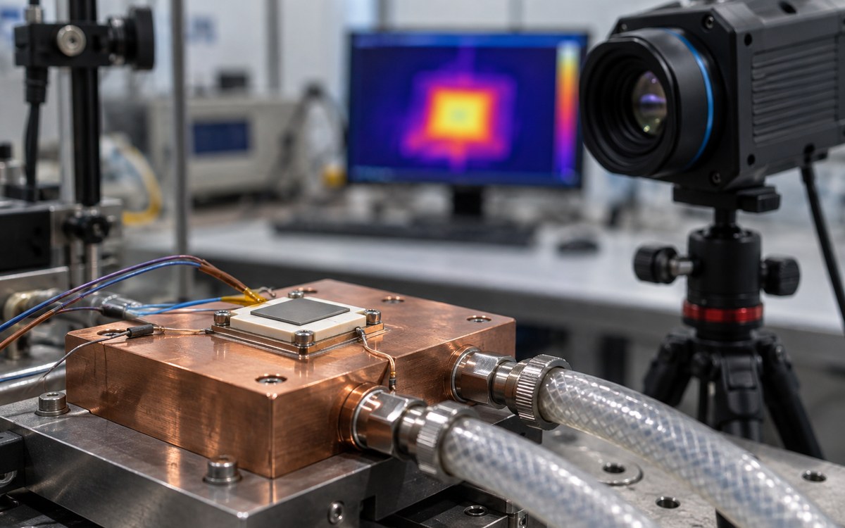
How Do Thickness, Area, and Heat-Source Size Affect Spreading?
The correct size is the geometry that spreads heat beyond the active source without adding unnecessary vertical resistance, unused area, cost, or assembly difficulty.
| Design variable | If it is too small or thin | If it is too large or thick | What sets the useful range |
|---|---|---|---|
| Thickness | Less cross-sectional area for lateral spreading and more handling risk | Longer vertical heat path, higher material cost, and more package height | Compare junction temperature and stress across manufacturable thicknesses |
| Footprint | Heat remains concentrated near the die | Outer area provides little benefit if it extends beyond the cooler contact zone | Match the useful footprint to the downstream contact area |
| Heat-source geometry | A uniform plate may not cover separated or elongated hot spots effectively | Extra material may sit outside the active heat-flow region | Size from the active power map, not the package outline |
A small, intense hot spot benefits more from lateral spreading than a device releasing the same total power over a broad area. One central die, several chiplets, and an elongated RF transistor may therefore need different spreader shapes even when their total power is similar.
Transient peaks also behave differently from continuous loading. The useful geometry depends on the power map and duty cycle, while the downstream cooler sets its practical limit. Area outside the cooler contact zone usually adds little value.
In practice, the useful geometry is the one that produces a favorable temperature and stress balance after bond layers, final cooling, flatness, mounting pressure, and manufacturing tolerances are included. A single “standard” diamond thickness cannot represent all of those conditions.
Why Do Metallization and Bonding Matter?
Bare diamond cannot simply replace a copper plate in every soldered assembly. Its surface often needs a compatible metallization system so it can be attached reliably to the die, substrate, package, or metal structure.
Metallization may use adhesion, barrier, wetting, and finish layers. Titanium, chromium, nickel, platinum, gold, and solderable alloys are among the systems used by specialist suppliers. The correct stack depends on the diamond surface, attachment alloy, process temperature, atmosphere, electrical requirements, and reliability target.
Poor interface design can cause several problems:
- weak adhesion between metal and diamond;
- incomplete solder wetting;
- excessive intermetallic growth;
- voids that increase local thermal resistance;
- cracking or delamination during thermal cycling;
- unintended electrical connection between top and bottom surfaces;
- die tilt or nonuniform bond-line thickness.
Flatness and surface roughness also matter. A nominally high-conductivity plate cannot perform as expected if only part of its surface makes effective thermal contact. Attachment pressure, solder volume, braze thickness, curing conditions, and fixture design all influence the finished interface.
Inspection should match the joint. Optical inspection may identify alignment and visible fillets but cannot prove internal bond quality. X-ray can help detect some void patterns in suitable structures. Acoustic microscopy, cross-sectioning, shear testing, thermal imaging, or transient thermal measurements may be required for development or qualification, depending on the package and acceptance criteria.
Metallization and bonding are therefore part of the heat-spreader system, not secondary assembly details. Their quality determines how much of the diamond’s material performance reaches the finished device.
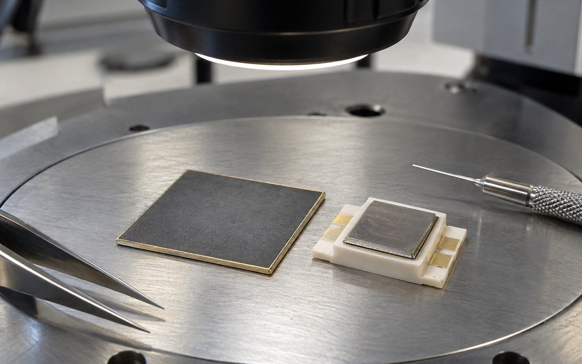
When Do AI Chips and Other High-Heat-Flux Applications Justify the Cost?
Diamond becomes commercially reasonable when local heat flux—not total system power alone—prevents a smaller, faster, or more reliable product, and conventional spreading solutions cannot meet the temperature target within the available space.
Recent industry attention has focused on artificial diamond because AI accelerators and other advanced processors continue to concentrate more computing power into dense packages. However, a large AI system does not automatically need diamond. The strongest candidates are packages in which localized junction temperatures, chiplet-to-lid spreading, memory proximity, or cooling-area constraints remain limiting after the conventional copper, vapor-chamber, interface, and cold-plate design has been optimized.
Applications where diamond spreading can be relevant include:
- AI accelerators, GPUs, ASICs, and other high-performance computing packages;
- RF and microwave power amplifiers with concentrated transistor heat sources;
- GaN and SiC power devices operating at high power density;
- laser diodes and high-power optical modules;
- satellite and aerospace electronics where mass and electrical isolation matter;
- compact power modules with strict junction-temperature or lifetime targets.
Cost is justified when the improvement changes a valuable system outcome. Examples include enabling higher device power, reducing peak junction temperature, improving temperature uniformity among dies, extending life, reducing package size, or lowering the burden on downstream cooling.
It is usually not justified when the real bottleneck is poor airflow, an undersized heat sink, an excessive thermal-interface gap, low mounting pressure, weak package contact, or heat generated across a large board area. Those problems should be corrected before specifying an expensive local spreader.
A meaningful comparison uses the same power map, boundary conditions, mechanical constraints, and temperature limits for an optimized conventional stack and the proposed diamond stack. Prototype thermal measurements then show whether the predicted improvement survives real interfaces and assembly variation.
How Should It Be Integrated with a PCB or Power Module?
In a PCB or power module, the diamond layer works as one part of the device-to-cooler heat path. Its effect depends on its physical position, both attachment interfaces, and the cooling structure that receives the redistributed heat.
Position in the thermal stack
The spreader may sit beneath a die, on a ceramic substrate, inside a package lid, or between a module and a larger cooling structure. A position close to a concentrated heat source gives it more opportunity to reduce local temperature gradients. If the largest temperature drop is instead in the PCB dielectric, thermal interface material, cold plate, or airflow path, the improvement from diamond remains limited.
Attachment to the surrounding structure
Diamond grade and thickness establish the available spreading performance. Flatness, surface roughness, metallization, attachment material, and bond-line thickness determine how much of that performance reaches the next layer. Electrical isolation, edge clearance, coplanarity, mounting load, and thermal-expansion differences also shape the finished interface.
Relationship with the PCB or module
An MCPCB or ceramic PCB still provides electrical interconnection and may conduct heat into a metal base. The diamond addresses a concentrated local hot spot; it does not replace copper distribution, thermal vias, dielectric selection, substrate thickness, attachment pressure, or external cooling. These elements continue to work together as one thermal structure.
Performance after assembly
Interface inspection can reveal voiding, alignment, or bond defects. Thermal measurements show whether the completed structure reduces junction or case temperature under the intended power map. Testing the diamond material alone cannot represent the performance of the assembled module.
Device-level measurements describe the package or module, while complete-system testing includes the final enclosure and cooling conditions. Both views are useful, but they answer different thermal questions.
EBest Circuit (Best Technology) can review the surrounding released PCB, ceramic PCB, MCPCB, and PCBA requirements, coordinate manufacturability at the board and assembly interfaces, and perform agreed inspection or testing within the approved production scope. Diamond grade, metallization, the device thermal model, package design, and final system-level thermal performance normally remain customer- or material-specialist inputs unless those activities are separately contracted.
FAQs About Diamond Heat Spreaders
Does a diamond heat spreader always perform better than copper?
No. Diamond offers much higher material conductivity, but the finished temperature also depends on spreader geometry, bond-line quality, package construction, and the downstream cooler. If another layer dominates the thermal resistance, replacing copper with diamond may produce only a limited improvement.
Is CVD diamond electrically insulating?
The diamond itself is electrically insulating. However, surface metallization, solder, brazing alloys, and surrounding package features may create conductive paths. Electrical isolation should therefore be evaluated for the complete assembled structure rather than inferred from the bare diamond alone.
When is copper-diamond more suitable than CVD diamond?
Copper-diamond is often more suitable for a larger lid, carrier, insert, or structural heat-spreading part that must integrate with a metal assembly. CVD diamond is generally better suited to a thin local spreader positioned close to a concentrated heat source.
Can a diamond heat spreader replace the external heat sink?
Usually not. The diamond spreads heat over a larger area, but a heat sink, cold plate, chassis, or other cooling structure must still remove that heat from the system. Both parts must be sized for the same power and operating conditions.
How should the thermal benefit be verified after assembly?
Compare junction or case temperature under the same power map, mounting conditions, and cooling boundaries used for the conventional design. Interface inspection and thermal measurements are both important because material data alone cannot reveal voiding, poor contact, or excessive bond-line resistance.
If you are evaluating how a customer-specified diamond heat spreader will interface with a PCB, ceramic substrate, MCPCB, or power-module assembly, send the released assembly data and thermal requirements to sales@bestpcbs.com. EBest Circuit (Best Technology) can review the surrounding board and assembly interfaces within the agreed manufacturing scope before you commit to the most expensive material.
You may also like




Tags: Copper-Diamond Heat Spreader, CVD Diamond Heat Spreader, Diamond Heat Spreader