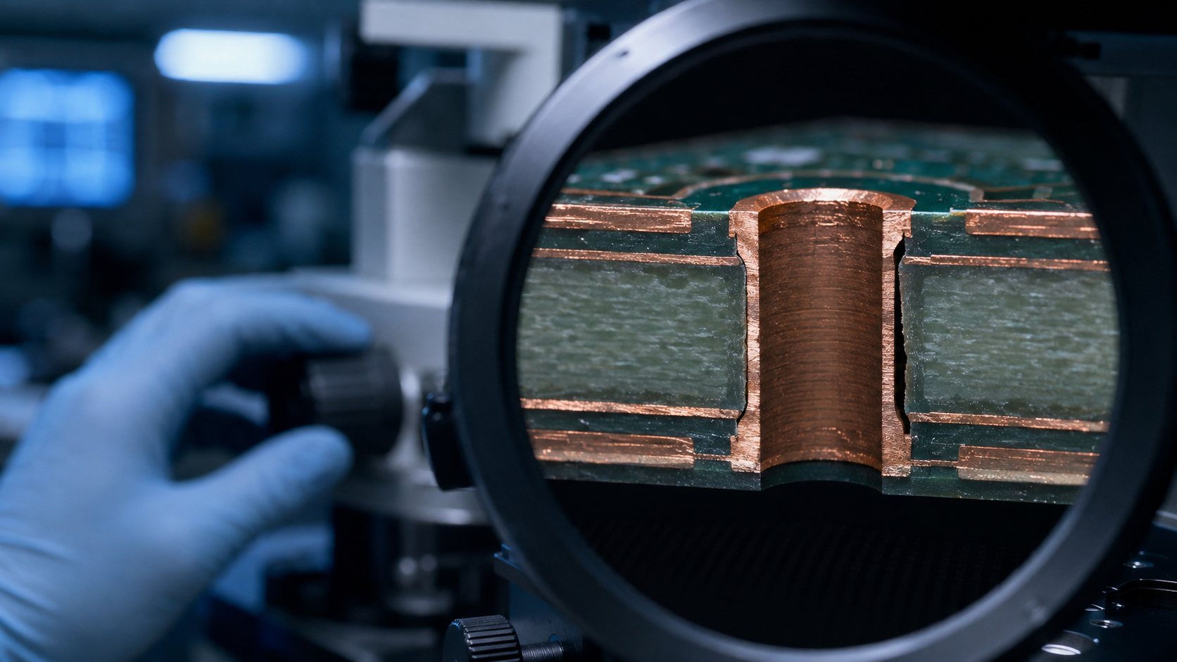
PCB hole wall pullaway is a separation between the plated copper barrel and the surrounding dielectric along a drilled hole. It is a cross-sectional finding, and it should not be diagnosed from a vague electrical failure or a top-view image. The first job is to confirm where the separation exists, whether it appeared before or after thermal stress, and whether other plated-through-hole defects are present.
A confirmed finding does not automatically prove one root cause or justify scrapping every board. Quality teams need representative samples, controlled microsection preparation, lot traceability and a cause-specific corrective-action plan. This guide gives designers, buyers and supplier-quality engineers a practical sequence for making that decision.
What PCB Hole Wall Pullaway Looks Like in Cross-Section
The characteristic feature is a visible gap at the interface between the plated hole copper and the resin/glass wall. The separation may be local or extend along part of the barrel. Its position, length, frequency and relationship to internal-layer connections should be recorded rather than reduced to a simple pass/fail label.
A useful micrograph shows the full hole, the affected interface and enough magnification to distinguish a true gap from polishing relief. The report should identify the board, lot, coupon or production location, section orientation, preparation condition and whether the specimen was thermally stressed.
Preparation artifacts can mimic separation. Excessive grinding pressure, poor specimen support, smeared resin, edge rounding or unsuitable etching can distort the interface. When the feature appears only on one questionable section, prepare another specimen before assigning a manufacturing cause.
Why Hole Wall Pullaway Matters After Thermal Stress
Pullaway matters because the plated barrel and dielectric experience different mechanical and thermal behavior, and loss of support can accompany a broader interconnect-reliability problem. The actual product risk depends on location, extent, associated cracks or voids, copper condition, end-use stress and the governing acceptance requirement.
A feature visible before stress points the investigation toward material condition, hole preparation, lamination and plating history. A feature that appears or grows after a defined thermal exposure may indicate that the interface could not tolerate the applied expansion and contraction. The test method, temperature profile, dwell, cycles and sample conditioning therefore belong in the evidence package.
Do not use one dramatic micrograph to generalize across a production lot. Sampling must cover relevant panel positions, hole sizes, constructions and process batches. Electrical continuity alone also cannot reveal every developing interface problem.
Hole Wall Pullaway vs Plating Voids, Barrel Cracks, and Hole Breakout
Similar-looking hole defects require different corrective actions, so classify the morphology before changing the process.
| Finding | Where it appears | Diagnostic clue | Primary review direction |
| Hole wall pullaway | Copper-to-dielectric interface | Gap follows part of the hole wall | Interface preparation, material and thermal history |
| Plating void | Within or missing from deposited copper | Discontinuous copper coverage rather than interface separation | Cleaning, activation and deposition/plating control |
| Barrel crack | Across plated copper | Fracture passes through the copper wall | Copper properties, thickness, geometry and thermal strain |
| Inner-layer separation | Barrel-to-inner-layer junction | Connection defect is concentrated at an internal pad | Desmear, etchback and interconnect formation |
| Hole breakout | Annular ring at a land | Drill position removes part of the surrounding pad | Registration, drill size and annular-ring design |
A board can contain more than one defect. Record each morphology independently. For broader context on how prepared sections reveal hidden features, see the PCB microsection analysis guide.
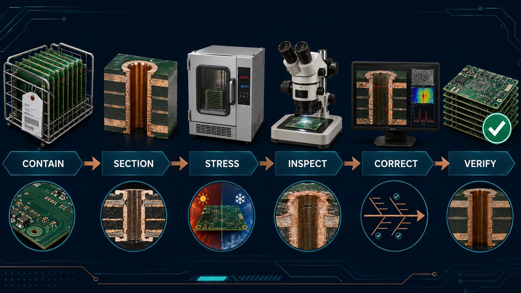
A Practical Failure-Analysis Sequence
Contain the lot first, preserve evidence, then test competing explanations in a controlled sequence.
- Contain: identify affected lots, panels, date codes and downstream assemblies without destroying evidence.
- Document: save failure symptoms, inspection images, test history and the exact acceptance concern.
- Sample: select suspect and known-good boards across relevant panel positions and hole structures.
- Section: prepare representative holes with controlled orientation and record pre-stress condition.
- Stress: apply only an agreed test profile when comparison after thermal exposure is needed.
- Inspect: measure and photograph the interface, barrel, inner-layer junctions and nearby laminate.
- Correlate: compare findings with material lots, lamination, drilling, desmear and plating records.
- Correct and verify: change the confirmed contributor, then validate with a controlled rebuild.
Need a second review of a plated-hole finding?
Send the stackup, drill table, material callout, lot history, micrographs and thermal-stress conditions. EBest Circuit can review whether the evidence supports a pullaway diagnosis and what additional data is needed before a rebuild.
Process Conditions That Can Contribute to Pullaway
Hole wall pullaway is usually investigated as an interaction among material condition, lamination, mechanical drilling, hole-wall preparation and later thermal exposure. A list of possible causes is not a root-cause report; each candidate must be matched to records and physical evidence.
| Process area | Condition to investigate | Evidence that helps |
| Incoming laminate and prepreg | Material condition, storage or construction variation | Material certificates, lot traceability and controlled comparison |
| Lamination | Resin flow, cure history or local stress around the hole structure | Press recipe, stack records and sections from multiple locations |
| Drilling | Smear, roughness, heat damage or tool wear | Tool count, hit count, feeds/speeds and unplated-hole inspection |
| Desmear and conditioning | Insufficient, excessive or nonuniform wall preparation | Chemistry control, dwell records and hole-wall morphology |
| Metallization and plating | Poor initial coverage or weak interface formation | Bath controls, deposition records and copper continuity |
| Thermal exposure | Stress beyond the qualified construction or repeated excursions | Assembly/rework profile, test profile and before/after sections |
Correlation is essential. If the finding clusters by one drill tool, panel region or material batch, that pattern is more useful than a generic assumption. If it appears across unrelated conditions, expand the investigation rather than forcing the first theory.
How Lamination, Drilling, and Desmear Interact
The plated interface is created by a chain of processes, so an upstream condition can alter how a downstream process behaves. Lamination establishes the resin/glass structure. Drilling exposes and mechanically modifies that structure. Desmear and conditioning remove residues and prepare the wall for metallization. Copper deposition and electroplating then build the conductive barrel.
A smooth-looking finished barrel does not prove every interface step was robust. Drill heat can change the surface that desmear must treat; excessive wall attack can create a different morphology; nonuniform conditioning can affect initial copper coverage. Later thermal stress may reveal a weak interface that was not obvious in an unstressed section.
Review the chain as one system. For an overview of the finished structure, compare the finding with the through-hole circuit board guide. For thermal evaluation context, the solder float test guide explains why test conditions and post-stress sections must be documented.
What to Check in the Microsection Report
A useful report lets another engineer understand the specimen, reproduce the interpretation and compare it with the agreed requirement. Ask for:
- board part number, revision, lot and panel or coupon location;
- hole type, nominal finished diameter and relevant layer connections;
- section orientation and whether the cut passes through the hole center;
- preparation and etching condition;
- overview and detail images with scale or magnification;
- location and extent of each interface gap;
- barrel, corner and inner-layer-junction observations;
- thermal conditioning or stress history;
- sample count and number of affected holes;
- acceptance reference and an explicit conclusion.
If the report only shows one cropped image without lot identity or test history, treat it as a lead for investigation, not a complete disposition record.
Containment Steps Before More Boards Are Built
Containment should prevent mixing, preserve traceability and collect enough evidence for a focused decision.
- Pause release of the suspect lot where the product risk justifies it.
- Separate suspect, screened, reworked and accepted material physically and in records.
- Record panel, lot, material, drill and process-batch relationships.
- Reserve untested samples before destructive analysis consumes the available evidence.
- Define the inspection or test used for temporary screening and acknowledge its limits.
- Notify assembly or product teams if additional thermal cycles could change the evidence.
- Agree who has authority to accept, rework, rebuild or scrap material.
Containment is not the permanent fix. A screen that finds obvious failures may still miss latent interface weakness, so do not close the issue until the corrective action is verified.
Corrective Actions Must Follow the Confirmed Cause
Changing several process settings at once can produce a passing sample without proving which change solved the problem. Link each action to an observed cause and a measurable verification result.
| Confirmed evidence | Corrective-action direction | Verification |
| Finding tracks a drill tool or wear interval | Review tool life, parameters, entry/backer system and maintenance limits | Controlled drill trial plus wall and plated-section comparison |
| Wall preparation is nonuniform | Restore chemistry, agitation, dwell and loading controls | Process-control data plus representative sections |
| Material/lamination batch correlation | Review storage, layup, press cycle and material compatibility | Traceable rebuild using controlled material and press records |
| Only excessive downstream thermal history correlates | Review assembly, rework and qualification profiles | Agreed thermal profile followed by section and continuity checks |
| Preparation artifact is confirmed | Correct specimen preparation and interpretation method | Repeat sections by an independent or controlled method |
A verification build should isolate the intended correction where practical and preserve the same evidence chain used to diagnose the failure.
Design and RFQ Information That Improves the Review
The fastest useful supplier review starts with controlled design data and failure evidence, not only a screenshot. Send:
- Gerber or ODB++ data and the released fabrication drawing;
- controlled stackup and material callout;
- NC drill files and drill table;
- finished-hole requirements and relevant acceptance class or customer specification;
- quantity, lot identity and affected panel positions;
- original micrographs, not only compressed report screenshots;
- sample preparation and thermal-stress details;
- assembly/rework profile if the finding occurred after PCBA processing;
- electrical symptom, field history and known-good comparison;
- required containment timing and target rebuild date.
For a new build, mark any special coupon, microsection or thermal-test requirement in the purchase package before quotation. Requirements added after fabrication may not be represented by retained samples.
Turn a defect image into a controlled review package
EBest Circuit can review your PCB data, hole structures, inspection requirement and production quantity together. Include the evidence above so engineering can separate immediate containment from the permanent corrective action.
Questions to Ask a PCB Supplier About the Finding
Ask questions that produce traceable evidence and decisions, not a generic assurance that the issue has been fixed.
- How was the pullaway distinguished from a preparation artifact or plating void?
- Was it present before thermal stress, after stress, or both?
- Which lots, panels, hole sizes, tools and material batches were compared?
- What evidence supports the proposed root cause?
- What material is contained, and how is its status identified?
- Which process control changed, and who approved it?
- How will the corrective action be verified on the next build?
- What records and samples will be retained?
If the issue is part of a broader supplier-quality investigation, use the same evidence discipline described in our guide to reducing PCB manufacturing defects.
FAQ About PCB Hole Wall Pullaway
Can hole wall pullaway be seen with visual inspection?
Usually not reliably. It is an interface feature inside a plated hole and is normally evaluated with a prepared cross-section. Surface inspection may identify a suspect area but cannot confirm the full barrel interface.
Is hole wall pullaway the same as a plating void?
No. Pullaway is separation at the copper-to-dielectric interface. A plating void is missing or discontinuous copper coverage. Both can exist in one hole, so the report must identify each morphology.
Does every pullaway indication require lot rejection?
Not automatically. Disposition depends on the governing requirement, the confirmed morphology, extent, sample evidence, associated defects, thermal history and product risk. The customer and responsible quality authority should make the documented decision.
Can microsection preparation create a false indication?
Yes. Poor support, grinding or polishing can produce edge relief and apparent gaps. Repeat preparation, additional samples and clear overview images help distinguish an artifact from a repeatable interface condition.
Should samples be checked before and after thermal stress?
When the investigation concerns thermal robustness, a controlled before/after comparison can be valuable. Record the exact conditioning and profile so the result can be interpreted and reproduced.
Can electrical testing rule out hole wall pullaway?
No. A hole may still conduct during a basic test even when an interface concern exists. Electrical results should be combined with cross-sectional and process evidence.
Is drilling always the root cause?
No. Drilling is one contributor to investigate, but material condition, lamination, hole-wall preparation, metallization and later thermal exposure can interact. Root cause requires correlation, not assumption.
What images should a supplier provide?
Ask for an overview of the full hole and detailed images of the affected interface, each with scale or magnification, specimen identity, orientation and stress condition.
What files should be sent for an engineering review?
Send fabrication data, drawing, stackup, material callout, drill files, acceptance requirements, lot traceability, original micrographs and the test or assembly thermal profile.
How is a corrective action verified?
Use a traceable rebuild or controlled trial that applies the cause-specific change, then repeat the agreed inspection and stress sequence on representative samples. A passing result without controlled inputs is weak evidence.
Final Decision Framework
A defensible decision answers four questions: Is the feature real, how widely is it present, what evidence supports the cause, and did a controlled rebuild verify the correction? If any answer is missing, keep the issue open or narrow the decision to temporary containment.
For new production, convert the lesson into explicit drawing notes, inspection requirements, sampling, retained evidence and supplier communication. That turns a one-time failure analysis into a repeatable control.
Request a PCB fabrication and failure-evidence review.
Send Gerber or ODB++, stackup, drill data, material callout, quantity, lot history, micrographs, thermal profile and required delivery date to sales@bestpcbs.com, or use the PCB quote form. EBest Circuit will review the available evidence and identify what must be confirmed before production or corrective rebuild.
You may also like






Tags: pcb failure analysis, PCB Quality Control, Plated Through Hole