An 2 layer PCB stackup looks simple, but it still affects board thickness, copper weight, routing space, grounding, impedance expectations, assembly yield, and final product fit. For engineers and buyers, the practical question is not only whether a board has two copper layers. It is whether the finished PCB can match the drawing, connector, enclosure, soldering process, and test requirement without avoidable rework.
EBest Circuit (Best Technology) supports 2 layer FR4 PCB fabrication, stackup review, copper thickness confirmation, surface finish selection, SMT assembly, inspection, testing coordination, and small-batch production. If your project already has Gerber files, ODB++, stackup notes, BOM, CPL, drawings, or assembly requirements, please send them to sales@bestpcbs.com for engineering review before production.
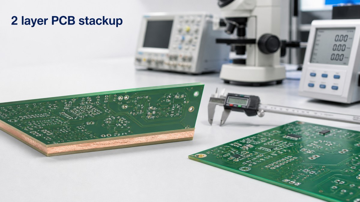
What Is a 2 Layer PCB Stackup?
A 2 layer PCB stackup is the layer structure of a printed circuit board with one copper layer on the top side and one copper layer on the bottom side. Between the copper layers, the board normally uses an insulating core material such as FR4. Solder mask, silkscreen, and surface finish are then added according to the production requirement.
In everyday quoting, buyers may also call this a double sided PCB, two layer PCB, or 2 layer circuit board. These terms are closely related, but the stackup is the part that tells the manufacturer how the board thickness, copper, dielectric material, and layer arrangement should be built.
A useful 2 layer PCB stackup should make these points clear:
- finished board thickness, such as 1.6 mm +/-10%;
- top and bottom copper weight, such as 1 oz or 2 oz;
- FR4 grade, high-Tg material, or other laminate requirement;
- surface finish, such as HASL, lead-free HASL, ENIG, OSP, or immersion silver;
- solder mask color and silkscreen requirement;
- controlled impedance or special routing notes, if required;
- SMT, through-hole, panelization, and test requirements.
Standard 2 Layer PCB Stackup Structure
A standard 2 layer PCB stackup is usually built with copper on both sides of an FR4 PCB core. The top layer may carry components, signals, power traces, and local ground copper. The bottom layer may provide additional routing, ground return paths, power routing, and connector connections.
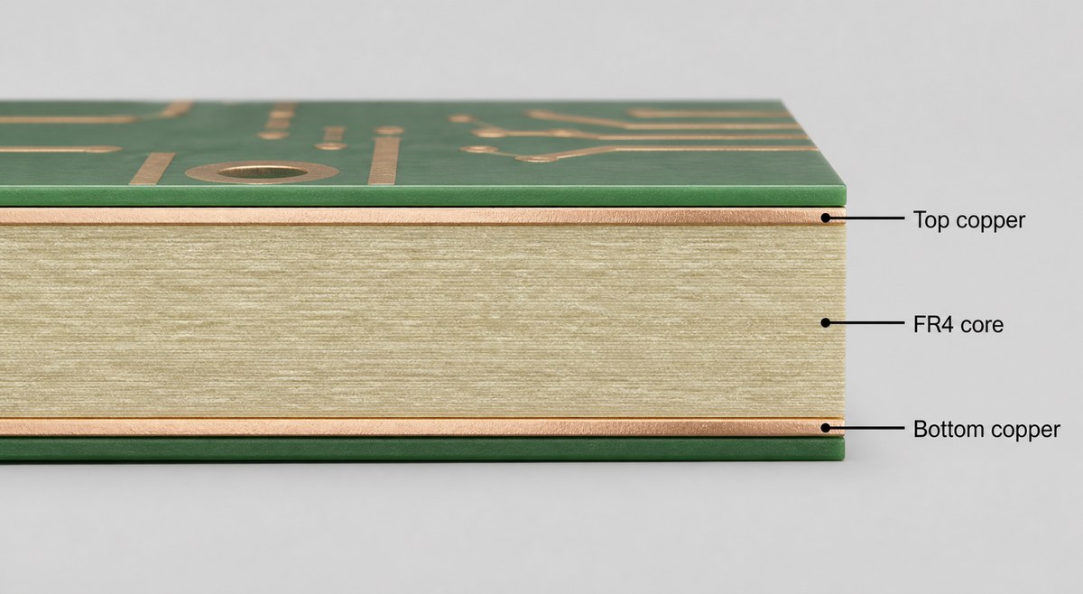
| Layer | Practical Role |
| Top solder mask | Protects copper and defines solderable openings |
| Top copper | Components, signals, power, or ground copper |
| FR4 core | Insulation and mechanical support |
| Bottom copper | Routing, return paths, connectors, or ground copper |
| Bottom solder mask | Copper protection and solder control |
The stackup may be simple, but the production result still depends on material availability, copper thickness, finished board thickness, drilling, solder mask registration, surface finish, and panelization. A two layer board should not be treated as a board with no engineering risk.
1.6mm 2 Layer PCB Stackup and Copper Weight
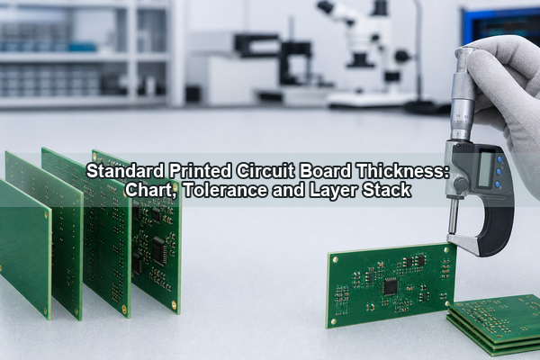
Many 2 layer PCB projects use a 1.6 mm finished board thickness because it is widely supported, mechanically stable, and compatible with many connectors and enclosures. However, 1.6 mm should refer to the finished board thickness, not only the raw laminate thickness.
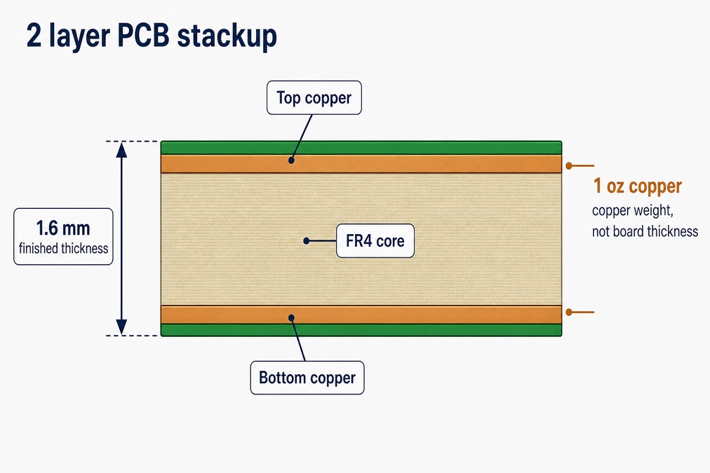
Copper weight is a different requirement. For example, 1 oz copper describes the copper thickness or copper weight used on the conductive layers. It does not mean the whole board is 1 oz thick. This distinction matters when a drawing includes both board thickness and copper thickness.
Before production, confirm these thickness-related details:
- finished board thickness and tolerance;
- top and bottom copper weight;
- whether copper is base copper or finished copper;
- surface finish requirement;
- connector or enclosure thickness limits;
- whether impedance or current capacity depends on the stackup.
2 Layer PCB Stackup for Signal, Power, and Ground Routing
A 2 layer PCB gives less routing freedom than a 4 layer board, so the signal, power, and ground strategy must be practical. If the board has simple low-speed signals, connectors, LEDs, sensors, or basic control circuits, a two layer structure may be enough. If the board has high-speed interfaces, dense BGAs, strict EMI requirements, or multiple power domains, the project may need more review.
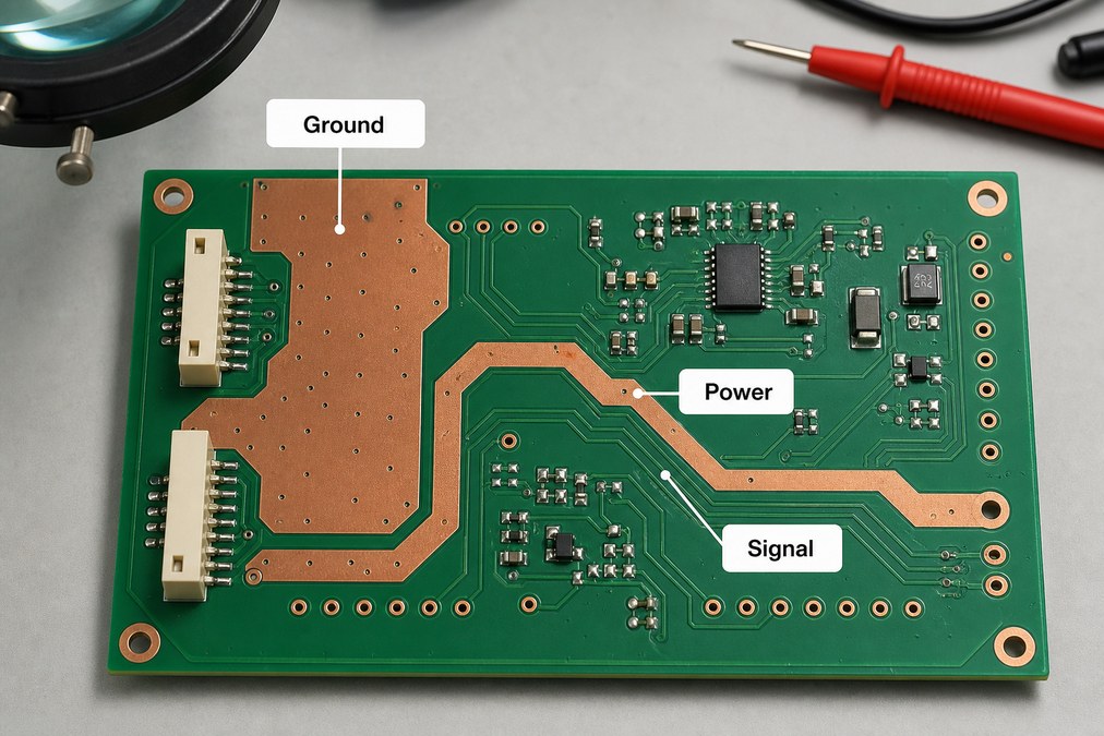
For many 2 layer boards, production review focuses on:
- return path continuity for important signals;
- wide enough power traces for current paths;
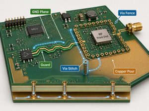
- clear ground copper and via stitching where needed;
- connector orientation and pin mapping;
- thermal relief, copper balance, and solderability;
- test points and inspection access after assembly.
The PCB manufacturer should not change the customer’s circuit intent. EBest Circuit can review whether the approved files are manufacturable and whether the stackup, copper, drilling, solder mask, and assembly notes are clear enough before production.
2 Layer PCB Stackup vs 4 Layer PCB Stackup
A 2 layer PCB stackup is often a good choice when the project needs a lower-cost board, simple routing, fast prototype validation, or a compact control board without strict high-speed requirements. A 4 layer stackup is usually considered when the board needs better power distribution, cleaner ground reference, controlled impedance, denser routing, or improved EMI behavior.
| Item | 2 Layer PCB | 4 Layer PCB |
| Layer structure | Top and bottom copper | Two outer layers plus inner planes |
| Routing space | Limited but cost-effective | More routing freedom |
| Ground reference | Depends on copper planning | Usually stronger with inner plane |
| Cost | Lower | Higher |
| Best fit | Simple to moderate circuits | Dense, faster, or noise-sensitive boards |
The right choice depends on the product, not only the layer count. If the 2 layer board can meet routing, grounding, thermal, and assembly needs, it may be the better commercial choice. If the board is already crowded or unstable, moving to 4 layers may save debugging time later.
Manufacturing Checks Before 2 Layer PCB Fabrication
A 2 layer PCB may be easier to manufacture than a high-layer-count board, but file review still matters. A small missing note can lead to wrong thickness, wrong surface finish, solder mask mismatch, connector fit problems, or assembly delay.
EBest Circuit typically checks:
- Gerber or ODB++ file completeness;
- drill file and plated-through-hole requirements;
- finished board thickness and tolerance;
- copper weight and current-related traces;
- minimum line width, spacing, annular ring, and solder mask opening;
- surface finish and solderability requirement;
- panelization, tooling holes, fiducials, and breakaway method;
- test requirement and outgoing inspection notes.
This review is useful because the buyer receives a finished PCB, not a file screenshot. The file must be translated into a real board that can be drilled, plated, etched, solder-masked, finished, tested, packed, and assembled.
SMT and PCBA Risks on 2 Layer PCB Boards
If the 2 layer PCB also needs SMT assembly, the stackup should be reviewed together with assembly data. Board thickness, panel size, component placement, solder mask openings, fiducials, and connector positions can all affect SMT yield. If the project also includes component sourcing, the BOM should be checked before SMT scheduling.
Before assembly, the useful files include:
- Gerber or ODB++ files;
- BOM with approved part numbers;
- CPL or pick-and-place file;
- assembly drawing;
- polarity and orientation notes;
- panelization drawing;
- testing and packing requirements.
For prototype and small-batch PCBA projects, EBest Circuit can review PCB fabrication and SMT assembly together. This helps keep board thickness, panelization, component sourcing, soldering, inspection, and packing notes visible under one workflow. This is especially useful when the project is still in prototype PCB assembly validation.
EBest Circuit 2 Layer PCB Stackup Manufacturing Capabilities
EBest Circuit supports 2 layer FR4 PCB projects from prototype to small-batch and production runs. The practical value is not only making a bare board, but helping the customer confirm the production path before the order moves forward.
| Requirement | EBest Circuit Support |
| Board type | 2 layer FR4 PCB and double sided PCB |
| Thickness review | Finished thickness and tolerance confirmation |
| Copper options | Common 1 oz or higher copper review by project |
| Surface finish | HASL, lead-free HASL, ENIG, OSP, and other options |
| Assembly | SMT, through-hole, mixed assembly, and inspection |
| Documents | DFM notes, stackup confirmation, test reports when required |
EBest Circuit (Best Technology) has worked in PCB and PCBA manufacturing since 2006 and serves customers in more than 40 countries and regions. For customers comparing suppliers, stable engineering communication is often as important as the quote itself, especially when the project needs both PCB fabrication and assembly.
2 Layer PCB Stackup Case Study for a Prototype Build
A USA customer needed a small-batch 2 layer PCB prototype for a compact control board. The board looked simple at first, but the project still had several details that could affect assembly and validation.
Project snapshot:
- Customer region: USA;
- Application: compact control and sensor interface board;
- Quantity: 50 pcs prototype build;
- PCB type: 2 layer FR4 PCB;
- Finished thickness: 1.6 mm +/-10%;
- Copper: 1 oz top and bottom copper;
- Surface finish: lead-free HASL;
- Assembly: SMT after PCB fabrication;
- Delivery focus: prototype validation before the next small batch.
What EBest Circuit reviewed before production:
- stackup, copper weight, board thickness, and solder mask notes;
- panelization method for SMT handling;
- BOM availability and approved part numbers;
- component polarity, connector direction, and placement data;
- electrical test before assembly and visual inspection after SMT;
- single-board packing after assembly to reduce handling damage.
The useful result for the customer was a clearer prototype path. The order quantity was small, but the board still moved through file review, PCB fabrication, SMT preparation, inspection, and packing as one controlled project. That is the kind of support that helps engineering teams validate a 2 layer PCB before scaling the design.
FAQs About 2 Layer PCB Stackup
1. Is a 2 layer PCB stackup the same as a double sided PCB?
In most PCB manufacturing contexts, yes. A double sided PCB usually means a 2 layer PCB with copper on both the top and bottom sides.
2. What is the standard thickness for a 2 layer PCB?
Many 2 layer FR4 boards use 1.6 mm finished thickness, but 0.8 mm, 1.0 mm, 1.2 mm, and other thicknesses may also be used depending on the product.
3. Is 1 oz copper the same as 1.6 mm PCB thickness?
No. 1 oz copper describes the copper layer weight or thickness. 1.6 mm describes the finished board thickness from the top surface to the bottom surface.
4. Can a 2 layer PCB stackup support controlled impedance?
Some 2 layer boards can support impedance requirements, but the stackup, trace width, dielectric thickness, copper thickness, and test requirement should be reviewed before fabrication.
5. What files should I send for a 2 layer PCB quotation?
Send Gerber or ODB++ files, drill files, stackup or thickness notes, BOM, CPL, assembly drawing, surface finish requirement, quantity, test notes, and packing requirements.
All in all, a 2 layer PCB stackup should be clear before production begins. If your project needs 2 layer FR4 PCB fabrication, thickness review, copper confirmation, SMT assembly, or prototype-to-small-batch support, please send your Gerber files, BOM, CPL, drawings, and project notes to sales@bestpcbs.com. EBest Circuit can help review the manufacturing and assembly path before your boards move into production.