





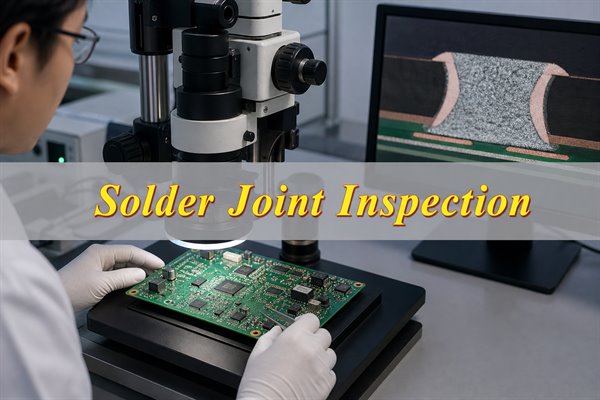
Solder joint inspection verifies whether each connection meets the specified workmanship and product-class requirements. A defensible plan combines documented criteria with visual inspection, SPI, AOI, X-ray and electrical testing. The goal is controlled, traceable evidence that the assembly meets its requirements, not a cosmetically perfect board.
What Is PCB Solder Joint Inspection and Why Is It Important?
PCB solder joint inspection examines paste deposits, formed joints and process evidence against defined criteria. A neat joint can still contain insufficient solder, poor wetting or a hidden void. A matte lead-free joint may be fully acceptable.
Effective inspection catches defects before they become field failures. It also provides objective evidence for lot acceptance, corrective action and traceability. Before production, define the assembly standard, product class, package risks and inspection stages. Assign clear authority for accepting, rejecting or escalating nonconforming results.
What Does a Good Solder Joint Look Like and Which Defects Should Be Rejected?
A good solder joint has the wetting, solder quantity, alignment and geometry required for its specific termination. There is no universal shape or shine.
Inspect the lead, land and solder together. Apply the criteria for that termination and product class. Surface finish, alloy and process affect appearance. Gloss alone does not prove solder joint integrity.
| Inspection Characteristic | Acceptable Evidence | Nonconforming or Review Condition | Engineering Significance |
| Wetting | Solder visibly wets the required land and termination surfaces | Nonwetting, dewetting or exposed areas beyond the applicable limit | Poor wetting can reduce mechanical and electrical integrity |
| Solder quantity | Enough solder to form the required connection without obscuring critical evidence | Insufficient or excessive solder, or solder balls outside the applicable acceptance limits | Both too little and too much solder can hide or create failure risks |
| Joint geometry | Termination position and fillet dimensions satisfy the applicable criteria | Lifted lead, severe misalignment, open joint, bridging, disturbed shape or inadequate clearance | Geometry affects contact, electrical clearance and load transfer |
| Surface condition | Surface is consistent with the alloy and process, without damaging cracks or contamination | Cracks, foreign material, overheating or exposed metal outside the applicable criteria | Surface anomalies can indicate process damage or reduced durability |
| Hidden structure | X-ray or other evidence shows acceptable hidden-joint formation where required | Suspected opens, bridging, head-in-pillow indicators, displaced solder or voiding beyond the agreed limit | Bottom-terminated packages cannot be fully judged from the board surface |
Do not create a local reject rule from a photograph alone. Confirm the termination type and use the specified magnification and lighting. Record the acceptance clause or approved customer criterion behind the decision.
What Solder Joint Inspection Criteria, Standards and Requirements Apply?
A solder joint should be accepted only against a documented requirement. The inspection plan must name the applicable standard, revision and product class. It should also identify the assembly drawing, customer additions, approved deviations and the order of precedence when requirements differ.
IPC J-STD-001 defines how soldered electrical and electronic assemblies are produced and controlled. It covers materials, process requirements and minimum end-product expectations. IPC-A-610 provides the visual acceptability criteria used to judge the completed assembly. These documents are normally applied together, but the purchase order or drawing must state the required revisions and whether Class 1, 2 or 3 applies.
Package-specific guidance helps engineers select suitable inspection evidence. IPC-7095 addresses BGA implementation, while IPC-7093 covers bottom-termination components such as QFNs. These documents support design, process and inspection planning. They do not replace the acceptance criteria specified by contract.
The acceptance check must match the joint geometry and what can actually be observed. Visible SMT joints are evaluated for alignment, wetting, solder quantity, bridging, disturbed solder and terminal damage. Through-hole joints also require checks of source- and destination-side wetting, barrel fill, lead protrusion and damage to the land, barrel or laminate.
Hidden joints require an inspection method that can produce the missing evidence. For BGA, QFN and LGA terminations, define the X-ray system, viewing angle, coverage and measurement method before inspection. The plan should explain how opens, bridges, void patterns, head-in-pillow indications and uncertain results will be reviewed or escalated.
Product-specific limits must be written into the acceptance plan. Do not apply one universal void percentage, fillet shape or solder-coverage limit to every package. Define the measured area, calculation method and local concentration rule, then relate each limit to the thermal, electrical or reliability risk it controls.
Every acceptance decision needs traceable evidence. Record the board or lot identity, reference designator, defect classification and supporting image or measurement. Also retain the governing requirement, inspection equipment or program revision, disposition, rework status and reinspection result.
How Do You Choose the Right Solder Joint Inspection Method?
Choose solder joint inspection methods by visibility, package geometry, process stage and escape consequence. No single method covers every defect. Map each credible failure mode to the least complex repeatable method.
| Method | Primary Application | Detectable Conditions | Primary Limitation |
| Human visual inspection | Accessible joints, first articles, low-volume builds and rework verification | Bridges, alignment, wetting and contamination | Operator-dependent; no hidden-joint view |
| SPI | Paste control before reflow | Volume, area, height and offset | Does not inspect the completed joint |
| AOI | High-throughput visible inspection | Presence, polarity, placement and bridges | Occlusion restricts coverage |
| X-ray | Hidden or complex solder structures | Open-joint signatures, bridges, voids and alignment | Does not prove electrical function |
| Electrical testing | Connectivity and functional behavior | Opens, shorts and circuit failures | Can pass a mechanically weak joint |
| Cross-section | Internal-structure validation and failure analysis | Joint geometry, internal interfaces, cracks and separation | Destructive; examines only the selected section |
| Dye-and-pry | BGA or LGA interface failure analysis | Dye indications at cracked or separated interfaces | Destructive; does not provide a metallographic cross-section |
For a new assembly, map package type, accessibility, process history and failure severity to the chosen method. Use solder joint testing only as complementary evidence. This makes coverage auditable and avoids paying for irrelevant inspection.
What Can Human Visual Inspection of Solder Joints Reliably Detect?
Human visual inspection can reliably detect accessible surface defects when the method is controlled. It works well for first articles, low-volume builds and rework verification. It also helps resolve borderline AOI calls.

- Confirm the acceptance basis: Verify the assembly revision, product class and applicable standard before inspection. Keep approved deviations and package-specific criteria at the workstation.
- Control the viewing conditions: Use clean optics, stable board support and repeatable illumination. Select magnification that shows the full joint and the required detail. Change the viewing angle when leads or nearby parts create shadows.
- Inspect in a fixed sequence: Scan the board by region and reference designator. Check every required location once before reviewing suspected defects. This method reduces missed joints and duplicate inspection.
- Evaluate joint formation: Check visible wetting, solder quantity, fillet shape and terminal alignment where applicable. Confirm that the lead or termination remains seated. Look for acceptable clearance from adjacent conductors.
- Find connection defects: Visual inspection can reveal bridges, visible opens and obvious insufficient or excessive solder. It can also find disturbed joints, lifted leads, solder balls and cracked surface fillets.
- Find placement defects: Check polarity, offset, skew, tombstoning, missing parts and damaged components. Confirm that the visible termination reaches its intended land.
- Find workmanship damage: Look for contamination, flux residue outside the allowed condition and foreign material. Inspect solder mask, lands and laminate for heat, handling or rework damage.
- Record objective evidence: Identify the board, lot and reference designator. Save a clear image with the viewing angle and useful scale. Record the defect category, acceptance clause and final disposition.
- Escalate hidden or uncertain conditions: Use X-ray for obscured BGA, QFN and LGA connections. Use electrical testing when function or continuity must be proven. Request cross-section analysis when internal structure or failure cause remains uncertain.
Appearance alone cannot prove electrical continuity or long-term reliability. Lead-free solder may appear matte without being defective. A shiny surface does not prove complete wetting. Validate the work instruction with known defects and periodic inspector-agreement checks.
How Do SPI and AOI Support Automated Solder Joint Inspection?
SPI measures solder paste before reflow. It identifies printing variation before that variation becomes a finished-joint defect.
AOI checks visible component and solder conditions after placement or soldering. It verifies whether the assembly result matches the controlled program and acceptance criteria.
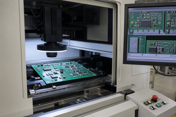
SPI measures paste height, area, volume, offset and shape. Repeated low volume can indicate a blocked aperture or poor paste release. Position drift can indicate board support, stencil alignment or printer setup problems.
AOI inspection in PCB assembly compares optical or 3D data with programmed limits. It checks component presence, polarity, position and visible solder features. It can also flag bridging, lifted leads, tombstoning and visible solder-volume anomalies.
SPI and AOI become more useful when their records are correlated by board and designator. Low paste volume followed by insufficient solder points toward printing. Acceptable paste followed by component offset points toward placement, board movement or reflow.
Control both programs by product revision and package type. Verify lighting, measurement repeatability and reference samples before production. Review false calls and escapes separately before changing inspection limits.
When Is X-Ray Solder Joint Inspection Required and What Hidden Defects Can It Detect?
X-ray solder joint inspection is needed when critical evidence is hidden from optical inspection. The inspection plan should state the target locations, method, coverage and acceptance basis.

- Hidden area-array packages: Use X-ray for BGA, LGA and bottom-terminated QFN joints. Optical inspection cannot see the complete connection beneath these packages.
- Obscured through-hole joints: Use X-ray when connectors, shields or board geometry hide required barrel-fill evidence. Do not infer internal fill from one visible surface.
- First-article validation: Inspect named high-risk packages before releasing the process. Compare the images with SPI, placement and reflow records.
- Production monitoring: Define full, sampled or risk-based coverage by board, package and designator. Increase coverage after a process change or adverse trend.
- Failure investigation: Use X-ray before destructive analysis when hidden opens, shorts or solder-distribution problems are suspected. Preserve the original images and machine settings.
- Bridges and missing solder: X-ray can show solder connections between adjacent features, missing balls and major solder-volume differences.
- Alignment and collapse: Compare ball position, diameter and shape across the package. Irregular patterns can indicate offset, uneven collapse, warpage or local thermal imbalance.
- Voids and solder distribution: Measure the defined joint or thermal-pad area with a controlled projection method. Record both total voiding and harmful local concentration when required.
- Open-joint indications: Look for separation, abnormal ball shape and inconsistent collapse. Head-in-pillow and nonwet opens may remain difficult to confirm in a top-down 2D image.
- Overlapping structures: Use oblique views, laminography or CT when copper planes and components obscure the target. Select the simplest method that resolves the required feature.
X-ray inspection for PCB assembly does not prove electrical function or metallurgical strength. Confirm ambiguous indications with electrical results, process history or destructive analysis. Record the view, settings, designator, finding and disposition.
How Should BGA, QFN, LGA and Through-Hole Solder Joints Be Inspected?
Match the inspection sequence to joint visibility and credible package failure modes. Begin with paste and placement evidence where available. Inspect the formed joint with the appropriate optical or X-ray method.
Use electrical testing as supporting evidence. It does not prove physical joint quality.
- BGA solder joint inspection: Review pre-reflow SPI. Then use 2D X-ray to check ball population, alignment, collapse, bridges and void patterns. Use oblique views or CT when structures overlap. Escalate irregular collapse or head-in-pillow indicators. Use electrical testing because X-ray alone does not prove connectivity.
- QFN solder joint inspection: Verify paste coverage and thermal-pad stencil segmentation before reflow. After reflow, check alignment and accessible perimeter evidence. QFN package guidance shows why standard cut flanks may not provide a reliable toe fillet. Use X-ray to check thermal-pad distribution, concentrated voiding, shorts and package lift. Apply the agreed void criteria.
- LGA inspection: Confirm paste uniformity and placement before the joints become hidden. Use X-ray after reflow to compare solder distribution, alignment, open-joint signatures, bridges and package tilt. Correlate anomalies with electrical results and reflow history; repeated location-specific defects require review of land geometry, coplanarity and thermal balance.
- Through-hole inspection: Inspect both sides for lead and land wetting, circumferential evidence, solder fill, protrusion, clearance, bridging and damage. When the barrel is obscured, use X-ray or approved destructive analysis rather than inferring fill from one surface. Reinspect reworked joints for lifted lands, plating damage and contamination.
For BGA soldering and other hidden terminations, record the inspected designators, viewing program, acceptance basis and disposition. This evidence is more useful than a generic “X-ray passed” statement.
What Steps Are Included in the Solder Joint Inspection Process?
A complete solder joint inspection procedure controls requirements, risk, equipment, disposition and corrective action. Each stage should leave enough evidence for another qualified person to reproduce the decision.
- Establish the acceptance basis: Confirm the drawing, BOM revision, workmanship standard and revision, product class, customer criteria and approved deviations. Resolve conflicts before inspection.
- Define the inspection population: Record the work order, board revision, lot size and inspected quantity. State whether coverage applies to every board, a defined sample, first articles or named critical locations.
- Map package and process risks: Identify hidden packages, fine pitch, high-current joints, thermal pads, selective-soldered connectors and reworked areas. Link each to credible defects and failure consequences.
- Select complementary methods: Match visual inspection, SPI, AOI, X-ray and electrical tests to defect visibility and risk. Reserve destructive analysis for validation or failure investigation. Document each method’s limitation.
- Verify inspection readiness: Check calibration, program revision, fixtures, lighting, magnification, X-ray settings and reference evidence. Run the approved verification routine before accepting production results.
- Inspect in process order: Review paste before reflow, visible conditions after soldering and hidden structures by X-ray. Record board ID, designator, method, defect code and supporting evidence during inspection.
- Control nonconforming findings: Segregate affected material, distinguish confirmed defects from ambiguous indications and preserve evidence. Only designated personnel should accept, reject, rework or escalate the result.
- Verify rework and lot impact: Reinspect with a method that can find the original defect, then check for rework damage. Determine whether the same mechanism may affect other units or locations.
- Close corrective action: Trend defects by package, location, machine, material and profile. Correct the verified cause, confirm performance on subsequent builds and update the control plan when improvement is sustained.
What Should Be Included in a Solder Joint Inspection Checklist and Report?
A useful solder joint inspection checklist identifies the product, acceptance basis, scope, evidence and disposition. The solder joint inspection report must make coverage traceable. A simple “pass” is not sufficient.
- Product and lot identity: Record part number, revision, work order, lot or serial IDs, lot quantity and inspected quantity.
- Acceptance requirements: State the standard and revision, product class, drawing requirements, customer additions and approved deviations.
- Inspection scope: Identify the process stage, locations, package groups, sample size, coverage level and methods. Distinguish full-board coverage from selected critical joints.
- Equipment and program control: Record equipment ID, calibration status, program revision, fixture and settings needed to reproduce the result.
- Finding details: Record board ID, designator, defect code, condition, severity, count and supporting image or measurement. Avoid vague descriptions such as “bad solder.”
- Result summary: State accepted, rejected, reworked and pending-review quantities. Separate confirmed defects, false calls and unresolved indications.
- Disposition and reinspection: Record the decision, rework authorization, reinspection method and result for each affected unit.
- Approval and traceability: Include the inspector, dates, disposition authority and attachment references. Retain the record for the required period.
Agree on the report format before ordering when traceability matters. Engineers should identify critical designators and hidden joints in the assembly data.
Procurement should confirm programming, sampled or 100% coverage, archived images and reinspection after rework.
What Determines Solder Joint Inspection Coverage, Sampling and Cost?
Solder joint inspection cost depends on risk, visibility, volume, evidence requirements and process capability. “100% inspection” is incomplete without the characteristics, method and stage. AOI of every board does not cover every hidden joint.
- Assembly risk: Safety, high-current and harsh-environment functions justify stronger evidence.
- Package mix: Hidden joints and dense layouts increase X-ray time and interpretation complexity.
- Build maturity: New products and unstable trends need greater initial coverage.
- Sampling basis: Lot size, history, capability, contract and escape consequence should drive the plan.
- Reporting depth: Archived images and serial-level traceability add labor and data handling.
- False-call burden: Poor programming increases review time without improving detection.
Ask suppliers to separate one-time programming or setup charges from recurring per-board inspection costs. For critical packages, confirm whether pricing includes every unit, a defined sample or only failure investigation.
How Can Inspection Results Prevent Recurring Solder Joint Defects?
Inspection prevents recurrence only when each finding is linked to a verified cause and controlled correction. Reject counts alone do not show where the process failed.
- Contain the affected population: Identify the lot, time window, line and component batches. Hold suspect material and increase inspection at the affected designators.
- Normalize the defect data: Report defects per board, joint or inspection opportunity. Separate true defects, false calls and unconfirmed indications.
- Stratify the pattern: Compare results by product, designator, package, printer, placement machine, oven profile and operator. A repeated location often indicates a local design or process cause.
- Confirm the failure mechanism: Use a second inspection method when the first result is ambiguous. Preserve samples for cross-section, dye-and-pry or other approved failure analysis when needed.
- Correct printing causes: For insufficient or excessive solder, check aperture design, stencil condition, paste handling, support and printer alignment. Verify the correction with SPI data.
- Correct placement causes: For offset, skew or tombstoning, check pickup accuracy, nozzle condition, placement force and land balance. Confirm component and PCB dimensional variation.
- Correct reflow causes: For non-wetting, opens or uneven BGA collapse, review the measured profile, alloy, surface condition and package warpage. Reprofile the actual assembly after a material or layout change.
- Correct through-hole causes: For low barrel fill, review flux application, preheat, contact time, solder temperature and thermal demand. Do not increase one setting without checking heat-sensitive parts.
- Validate effectiveness: Inspect a defined number of subsequent boards using the method that detected the original defect. Check that the correction did not create a different failure mode.
- Lock the improved process: Update programs, work instructions, control limits and training. Continue trend review until the improvement remains stable across normal production variation.
The corrective-action record should connect the defect, evidence, root cause, change and verification result. This record prevents teams from investigating the same problem without its history.
FAQs About Solder Joint Inspection
Q1: What should happen when AOI and X-ray results disagree?
A1: Hold the material and review what each method measured. Check the images, limits, package geometry and electrical result. Use higher-resolution or destructive analysis if risk remains unresolved.
Q2: Should solder joints be inspected before conformal coating or underfill?
A2: Yes, inspect before materials obscure access. Record the result and control any later rework.
Q3: Can X-ray inspection damage electronic components?
A3: Validated production exposure is normally nondestructive, but dose still requires control. Radiation-sensitive devices and repeated scans need component-specific review. Define exposure settings and limits before inspection.
Q4: Can a golden board replace written acceptance criteria?
A4: No. A golden board can support program verification but cannot replace the specified standard and customer requirements. It may contain variation that should not become a new acceptance limit.
Q5: When should inspection limits be revalidated?
A5: Revalidate after changes that can alter the joint or its image. Examples include component, PCB, stencil, alloy, equipment, program or reflow changes. Recurring false calls also require review.
Q6: Does successful reflow of a failed joint prove the original root cause?
A6: No. Recovery after reheating is evidence, not proof. Reflow changes solder, flux and mechanical contact. Preserve electrical data and images before repair, then investigate the original process conditions.
Q7: How can consistency between inspectors be checked?
A7: Use qualified samples and periodic attribute-agreement studies. Compare decisions by defect type, then retrain or clarify criteria where agreement is weak.
Q8: Why can an intermittent solder joint pass a room-temperature electrical test?
A8: A static test may not reproduce thermal or mechanical movement. Use controlled hot, cold, vibration or flex testing when service conditions justify it. Monitor the affected circuit while stress is applied.
Q9: Can inspection images from different systems be compared directly?
A9: Only when scale, angle, lighting or X-ray settings and image processing are controlled. Otherwise, apparent differences may come from the imaging setup rather than the joint.
Q10: Should inspection thresholds be relaxed to reduce false calls?
A10: Not without validation. Review the false-call cause, confirm known defects remain detectable and approve the revised limit before production use.
Need a PCBA quotation with a defined solder joint inspection plan? Send Gerber or ODB++, BOM, pick-and-place data, assembly drawings, quantity and product class. Include critical joints, testing requirements and traceability expectations.
EBest Circuit can review your inspection scope and prepare a practical quotation. Send the project package to sales@bestpcbs.com.
You may also like







Tags: solder joint inspection, solder joint inspection checklist, solder joint inspection criteria, x ray solder joint inspection