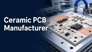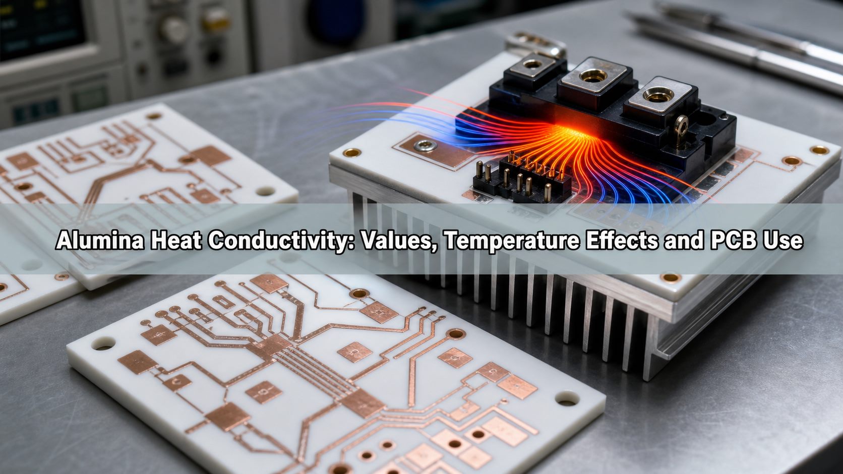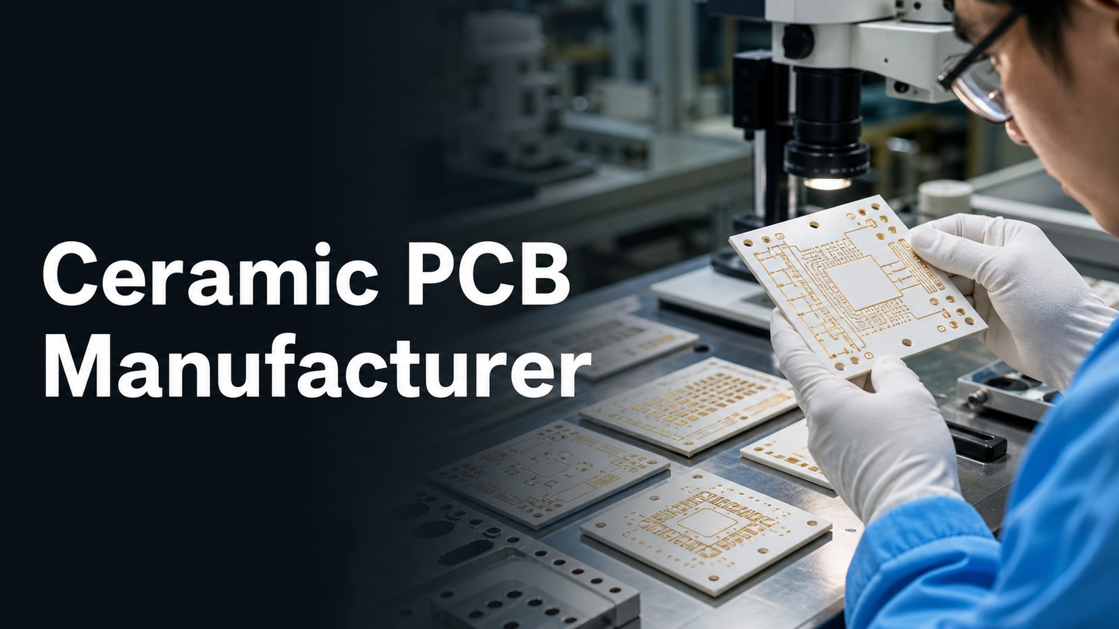
A ceramic PCB manufacturer should be selected by substrate material, metallization process, line and space capability, thermal reliability, inspection scope and RFQ clarity, not by the word ceramic alone. Alumina, aluminum nitride, DBC, DPC, AMB, thick film and thin film ceramic boards solve different engineering problems.
This guide is for engineers and purchasing teams comparing ceramic PCB suppliers for heat-critical, compact, high-temperature, power, LED, RF or sensor projects. It explains what the current supplier options show, what to verify in a supplier and what files to send before asking for price or lead time.
Ceramic PCB Manufacturer at a Glance
Choosing a ceramic PCB manufacturer means matching the process to the application before comparing prices. A supplier may be strong in DBC ceramic substrates but not the best fit for thin film precision work, AMB power modules or LTCC multilayer structures.
| Buyer decision | What to confirm | Why it matters |
|---|---|---|
| Material | Al2O3, AlN, ZrO2, Si3N4 or other ceramic substrate | Thermal conductivity, insulation, CTE and cost change by material. |
| Process | DPC, DBC/DCB, AMB, thick film, thin film, LTCC or HTCC | Each process supports different copper, line width and reliability needs. |
| Geometry | Panel size, thickness, hole size, trace/space and profile tolerance | Ceramic boards are not designed like standard FR4 PCBs. |
| Surface finish | OSP, ENIG, immersion silver or process-specific metallization | Finish affects solderability, bonding and assembly. |
| RFQ data | Drawing, substrate, copper or conductor thickness, quantity and test needs | Complete files reduce quote revisions and feasibility risk. |
Is Your Ceramic PCB Project Limited by Material or Thermal Uncertainty?
Ceramic PCB buyers need early review of substrate, metallization, heat path, assembly conditions and inspection needs.
| Customer Pain Point | Project Risk | How bestpcbs Helps |
|---|---|---|
| Substrate choice is not tied to the application | Thermal, insulation or mechanical expectations may not match the final board | bestpcbs asks for application environment, material expectations and thermal requirements before confirming the route. |
| Metallization or copper details are unclear | Cost, solderability and reliability can change with process assumptions | bestpcbs reviews drawings, surface finish, conductor requirements and assembly needs before quoting. |
| Dimensional tolerance is not defined | Fit, mounting or module assembly may be affected | bestpcbs checks drawings and tolerance notes with the fabrication data. |
| Testing scope is not specified | A high-reliability board may ship without the checks the application needs | bestpcbs confirms electrical, visual and project-specific inspection requirements during RFQ review. |
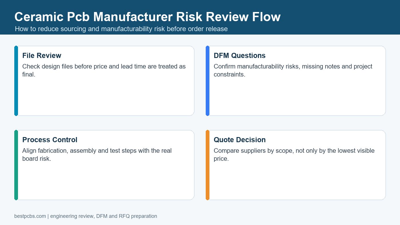
Ceramic PCB Buyer Priorities Before Supplier Selection
Ceramic PCB buyers should confirm substrate type, metallization, thermal requirements, assembly conditions, dimensional tolerance and inspection needs before choosing a supplier. Ceramic boards are often selected for heat, insulation or high-reliability reasons, so assumptions must be made explicit.
Share the application environment, thermal path, copper or metallization notes, component attachment method, operating temperature and test expectations. This helps the supplier review the board as a performance part instead of a generic PCB.
When Ceramic PCB Is the Right Choice
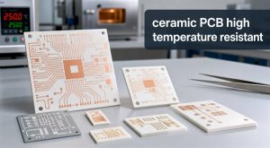
Ceramic PCB is the right choice when thermal conductivity, electrical insulation, high-temperature stability, dimensional stability or material reliability matter more than the cost advantage of FR4. It is often considered for power electronics, LED modules, RF circuits, sensors, high-temperature devices and compact thermal designs.
Bestpcbs has a dedicated ceramic PCB product page covering ceramic circuit boards such as alumina PCB and AlN ceramic PCB. The useful RFQ question is which ceramic material and process fit the design, not whether the project can be labeled as ceramic PCB.
Ceramic PCB Materials Buyers Should Compare
Ceramic PCB material selection should be driven by heat, insulation, CTE, strength, dielectric behavior and cost target. The capability files list ceramic substrate options such as Al2O3, AlN, ZrO2 and Si3N4 in the ceramic PCB capability sheet, with additional special-material notes in the original ceramic process file.
| Material family | Common buyer reason | RFQ note |
|---|---|---|
| Al2O3 alumina | Balanced insulation, heat resistance and cost | State purity or grade when specified by the design. |
| AlN aluminum nitride | Higher thermal performance than many standard ceramic options | Confirm process, substrate thickness and finish. |
| ZrO2 zirconia | Special mechanical or insulation needs | Use only when the application requires it. |
| Si3N4 silicon nitride | Strength and thermal reliability in demanding modules | Confirm with the supplier before quoting. |
DPC, DBC, AMB, Thick Film and Thin Film Differences
Ceramic PCB processes are not interchangeable; the process affects copper thickness, line precision, panel size, substrate choice and reliability testing. The RFQ should name the target process or ask the supplier to recommend one based on the electrical and thermal goal.
| Process | Typical fit | Buyer check |
|---|---|---|
| DPC ceramic PCB | Precision plated copper on ceramic | Review trace/space, conductor thickness and pad needs. |
| DBC/DCB ceramic PCB | Direct bonded copper substrates for power modules | Check copper thickness, substrate and thermal stress requirements. |
| AMB ceramic PCB | High-reliability power and thermal applications | Confirm material, copper thickness and test plan. |
| Thick film ceramic PCB | Printed conductor or functional paste circuits | Check conductor material and firing requirements. |
| Thin film ceramic PCB | Fine features and precision circuits | Check line precision, finish and inspection criteria. |
For process-specific context, see the bestpcbs DPC ceramic PCB, DCB ceramic PCB and AMB ceramic PCB pages.
Capability Ranges to Verify Before Quoting
Capability ranges should be verified against the exact ceramic process, because one ceramic PCB process does not share all limits with another. The original capability files show separate values for thin film, DBC/DCB, DPC and AMB ceramic PCB.
| Capability item from process files | Verified reference point | How to use it |
|---|---|---|
| Layer count | Thin film up to 10 layers; DBC/DCB, DPC and AMB listed as 2 layers in the English capability sheet | Confirm if a multilayer ceramic route is needed. |
| Max panel size | Examples include 200 x 200 mm for thin film and smaller listed sizes for DBC/DCB, DPC and AMB | Send drawing and panel needs for review. |
| Conductor thickness | Ranges differ by process, from micrometer-scale thin film to oz-level DBC/AMB copper | Do not compare quotes without the same conductor target. |
| Trace and space | Minimum trace/space differs by process; DPC and thin film allow finer values than AMB in the sheet | Mark critical features in the drawing. |
| Thermal stress test | The sheet lists process-specific thermal stress tests such as 350 C or 280 C conditions | Ask which test applies to the selected process. |
Design and DFM Checks for Ceramic PCB
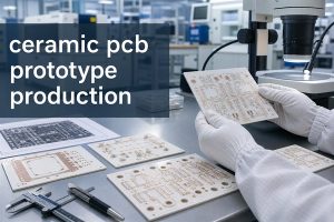
Ceramic PCB DFM review should happen before the supplier quotes final price because ceramic boards use different design rules from FR4. Brittle substrates, thermal expansion, metallization, profile tolerance and soldering method need early review.
- Confirm substrate type, thickness and final board outline.
- Review minimum trace/space and pad size for the chosen process.
- Check hole diameter, hole tolerance and whether PTH is required.
- Define solder mask opening, bridge and conductor surface requirements.
- Review heat source, mounting method, thermal interface and assembly load.
- Use the DCB ceramic PCB design guide when the project uses DBC/DCB ceramic technology.
Surface Finish and Metallization Decisions
Surface finish and metallization must match the process, component attachment method and reliability target. The ceramic capability files include surface finish references such as OSP, ENIG and immersion silver for several ceramic processes, while other ceramic methods may use process-specific metallization systems.
Do not choose finish only by price. Ask whether the board needs wire bonding, soldering, high-temperature exposure, low contact resistance, corrosion resistance or a specific assembly process.
Ceramic PCB Assembly and Component Sourcing
Ceramic PCB assembly should be planned with fabrication because the substrate, thermal mass, pad finish and component package can affect soldering and reliability. A separate assembly supplier may miss ceramic-specific risks if the fabrication assumptions are not shared.
For projects that require mounted components, send BOM, CPL, assembly drawings, polarity notes, thermal interface information and test requirements with the fabrication files. Bestpcbs can connect ceramic board fabrication with PCBA and PCB assembly service when the project needs a combined review.
Testing and Quality Control for Ceramic Circuit Boards
Testing should be selected according to process risk, not copied from a standard FR4 checklist. Ceramic PCB inspection can involve electrical continuity, isolation, profile tolerance, surface finish, hole position, thermal stress, solderability and application-specific checks.
| Quality item | What to define | Why it matters |
|---|---|---|
| Electrical check | Continuity, isolation and netlist requirements | Confirms the circuit matches design data. |
| Dimensional inspection | Outline, hole position, thickness and tolerance | Ceramic parts may have tight mechanical fit needs. |
| Thermal stress | Process-specific stress test or customer test condition | Supports high-heat application confidence. |
| Assembly inspection | AOI, solder joint, wire bond or special attachment checks | Assembly risk depends on finish and package type. |
What Determines Ceramic PCB Cost?
Ceramic PCB cost depends on substrate material, process route, conductor thickness, line precision, panel size, hole features, surface finish, testing and quantity. A supplier cannot quote accurately from the keyword alone.
The ceramic PCB price guide explains cost factors in more detail. For this manufacturer selection page, the key point is to keep every supplier quoting the same material, process, thickness, finish, testing and assembly scope.
How to Compare Ceramic PCB Manufacturers
Compare ceramic PCB manufacturers by process fit, engineering review quality, evidence of capability and quote transparency before comparing lead time or unit price. A good supplier should ask which ceramic technology the design needs and why.
- Can the supplier support the required substrate and process route?
- Do they explain DPC, DBC/DCB, AMB, thick film and thin film tradeoffs?
- Can they review trace/space, conductor thickness, holes and surface finish?
- Do they define thermal stress, inspection and acceptance criteria?
- Can they support assembly or component sourcing if PCBA is required?
- Do they avoid unsupported claims about universal capability or guaranteed lead time?
Files to Prepare for a Ceramic PCB RFQ
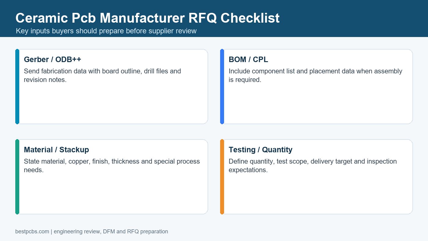
A complete ceramic PCB RFQ should include both circuit data and the application reason for selecting ceramic material. That lets the supplier recommend the right substrate and process instead of guessing from incomplete files.
- Gerber or ODB++ fabrication data and drill files.
- Mechanical drawing with outline, thickness, holes and tolerance.
- Target substrate such as Al2O3, AlN, ZrO2 or Si3N4 if already selected.
- Preferred process: DPC, DBC/DCB, AMB, thick film, thin film, LTCC or HTCC.
- Conductor thickness, surface finish, pad requirements and critical trace/space.
- Thermal, electrical, insulation, bonding or soldering requirements.
- BOM, CPL and assembly drawing if PCBA is required.
- Quantity, revision, target lead time and test or report requirements.
Common Ceramic PCB Sourcing Risks
The most common ceramic PCB sourcing risk is choosing a supplier before the substrate, process and reliability target are clear. That creates quote revisions, unsuitable material choices, avoidable failures and late production changes.
- Do not treat all ceramic PCB processes as interchangeable.
- Do not compare DBC pricing with DPC or thin film pricing without scope control.
- Do not send only Gerbers when material, thermal and test requirements matter.
- Do not assume FR4 design rules apply to ceramic substrates.
- Do not accept broad capability claims without process-specific confirmation.
Frequently Asked Questions About Ceramic PCB Manufacturers
What does a ceramic PCB manufacturer do?
A ceramic PCB manufacturer fabricates circuit boards or substrates using ceramic materials such as alumina, aluminum nitride, zirconia or silicon nitride. Depending on the process, the supplier may support DPC, DBC/DCB, AMB, thick film, thin film, LTCC or HTCC ceramic circuits.
Which ceramic PCB process should I choose?
Choose the process based on thermal load, conductor thickness, line precision, substrate material, assembly method and reliability requirement. If unsure, send the application notes and ask the supplier to compare DPC, DBC/DCB, AMB, thick film or thin film options.
Can ceramic PCB support assembly?
Yes, but assembly requirements should be reviewed early. Ceramic substrates, metallization, surface finish and thermal mass can affect soldering, bonding, inspection and test planning. Send BOM and CPL with the fabrication files.
Why is ceramic PCB more expensive than FR4?
Ceramic PCB usually costs more because the substrate, metallization, processing, tolerance control and testing are more specialized. The cost can be justified when thermal, insulation, high-temperature or reliability needs cannot be met by standard FR4.
Final RFQ Recommendation
Before selecting a ceramic PCB manufacturer, define the substrate, process route and application risk clearly enough for a real engineering review. A useful supplier comparison should use the same files, material assumptions, finish, tolerances, testing scope and assembly requirements.
For a ceramic PCB quote, send Gerber or ODB++ files, drill data, mechanical drawings, target substrate, process preference, conductor thickness, surface finish, thermal and insulation requirements, BOM, CPL, assembly drawings, quantity, testing requirements and target lead time to sales@bestpcbs.com. Best Technology / bestpcbs can review the files, confirm which ceramic process needs project-specific checking and help prepare the build as a ceramic substrate, assembled PCBA or production RFQ.