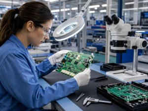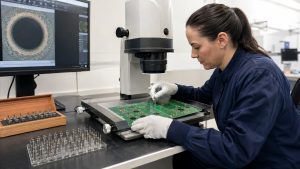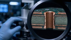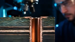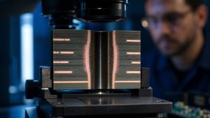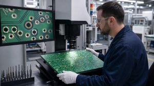
AOI in PCB manufacturing means automated optical inspection: a camera-based inspection process used to find visible defects on bare PCBs or assembled PCBAs before they move to the next production step. It helps manufacturers catch issues such as missing components, wrong polarity, solder defects, bridging, insufficient solder, misalignment, surface damage, and certain pattern defects, but it does not replace every electrical, X-ray, or functional test.
This guide explains where AOI fits in PCB and PCBA quality control, what it can detect, what it cannot prove, and what buyers should ask before sending an RFQ for production or assembly.
AOI in PCB Manufacturing at a Glance
AOI is a fast visual inspection method that compares PCB or PCBA images against programmed inspection rules. It is useful because many defects are visible before the board reaches final testing.
| Inspection point | AOI can help check | AOI cannot fully replace |
|---|---|---|
| Bare PCB | Pattern defects, solder mask issues, surface contamination, open or short risk clues | Full electrical testing and final acceptance criteria |
| SMT assembly | Missing parts, wrong polarity, offset, tombstoning, visible solder defects | Hidden solder joint X-ray or powered functional testing |
| Final PCBA | Visible assembly defects and workmanship consistency | Firmware, load, signal, thermal, or application-specific tests |
Where AOI Fits in the PCB Production Flow
AOI is usually placed after a manufacturing or assembly step where visible defects should be caught before more value is added to the board. In SMT assembly, AOI is commonly used after solder paste and reflow-related steps depending on the process plan. In bare PCB manufacturing, optical inspection can help flag pattern or surface issues before later processing.
For buyers, the important question is not simply whether AOI exists. Ask where it is used, which defect types are checked, and whether findings are reviewed by trained staff before boards are released.
What AOI Can Detect on PCBAs
AOI is strongest at detecting visible component and soldering problems on assembled boards. It is especially useful when there are many SMT parts and manual visual inspection would be slow, inconsistent, or easy to miss.
- Missing, shifted, skewed, or rotated components
- Wrong polarity on LEDs, diodes, ICs, or capacitors when markings are visible
- Solder bridges and visible insufficient solder
- Tombstoning, lifted leads, and package placement issues
- Surface contamination or visible damage
For assembled projects, AOI should connect with the broader PCBA service workflow rather than standing alone as a checkbox.
What AOI Can Detect on Bare PCBs
For bare boards, optical inspection can help identify visible pattern, solder mask, silkscreen, and surface issues before shipment or assembly. It may flag scratches, contamination, missing features, copper pattern problems, solder mask misregistration, or visual abnormalities that need review.
AOI is only one layer of control. Bare-board electrical testing, process control, material verification, and final inspection still matter, especially for boards with fine features, controlled impedance, high current, or special materials.
AOI vs SPI, X-Ray and Functional Testing
AOI checks visible features, SPI checks solder paste, X-ray checks hidden structures, and functional testing checks whether the circuit works under defined conditions. These tests answer different questions.
| Method | Best for | Typical limit |
|---|---|---|
| SPI | Solder paste volume and print quality before placement | Does not prove final component function |
| AOI | Visible placement and solder defects | Cannot see every hidden joint or prove circuit function |
| X-ray | BGA, QFN, hidden solder joints, voiding review | Not usually needed for every simple board |
| Functional test | Power, signal, firmware, application behavior | Requires buyer-defined test plan or fixture |
AOI Limits Buyers Should Understand
AOI reduces visual defect risk, but it does not guarantee that every board will pass electrical or application testing. It depends on the inspection program, image quality, board design, component markings, operator review, and whether the defect is visible to the camera.
Hidden BGA solder joints, internal layer issues, marginal electrical behavior, thermal performance, firmware problems, and intermittent failures may require other test methods. Buyers should define the risk level and ask which inspection combination is appropriate.
How AOI Supports DFM and Process Feedback
AOI findings can feed back into DFM and process improvement when recurring defects point to pad design, stencil, placement, soldering, or component issues. If the same defect appears repeatedly, the supplier should not only sort boards. They should investigate the cause.
Examples include solder bridging caused by pad spacing, tombstoning caused by land pattern imbalance, weak polarity markings, or recurring placement offsets. This is why quality control should connect to engineering review before repeated production.
AOI for SMT, Through-Hole and Mixed Assembly
AOI is most common in SMT inspection, but mixed assemblies still need a planned inspection approach. Through-hole parts, connectors, large components, and hand-soldered features may need visual inspection, selective process checks, or functional testing in addition to AOI.
For through-hole-heavy projects, review the assembly route and inspection plan before quoting. The through-hole assembly page can be useful when a project combines SMT and mechanical-strength components.
What Buyers Should Ask About AOI Before RFQ
Buyers should ask what AOI checks, when it is used, what defect criteria apply, and what other tests are needed for the product. A supplier that only says “AOI included” has not given enough information for a high-risk board.
- At which production stages is AOI used?
- Which defect types are programmed for this board?
- Are AOI findings reviewed before release?
- Does this board need X-ray because of BGA, QFN, or hidden joints?
- Does the buyer need to provide firmware, fixtures, or functional test requirements?
Cost and Lead-Time Impact of AOI
AOI can add inspection steps, but it often reduces downstream rework risk for assemblies with many components or visible soldering risk. The impact depends on board complexity, production volume, inspection program setup, and whether other tests are also required.
For quote planning, include test and inspection expectations early instead of adding them after the price is approved. The custom PCB cost guide can help buyers understand why inspection and testing should be treated as cost factors, not afterthoughts.
RFQ Checklist for AOI and PCB Quality Control
An RFQ should define the board files, assembly files, component risk, and inspection expectations clearly enough for the supplier to recommend the right quality plan.
- Gerber or ODB++ files and drill data
- BOM and CPL if assembly is required
- Assembly drawing, polarity notes, and test point requirements
- Package types such as BGA, QFN, fine-pitch ICs, connectors, or LEDs
- Required inspection: AOI, X-ray, electrical testing, programming, or functional testing
- Acceptance criteria and known product risks
Frequently Asked Questions
What does AOI mean in PCB manufacturing?
AOI means automated optical inspection. It uses cameras and programmed inspection rules to identify visible defects on bare PCBs or assembled PCBAs.
Can AOI replace functional testing?
No. AOI checks visible defects. Functional testing checks whether the circuit works under defined electrical or application conditions. Many projects need both.
Is AOI needed for every PCB assembly?
Not always. It is most valuable when there are many SMT components, fine-pitch packages, polarity-sensitive parts, or higher reliability requirements. Simple boards may need a lighter inspection plan.
Does AOI find BGA solder defects?
AOI can inspect visible features around BGA placement, but hidden solder joints usually require X-ray or another suitable inspection method.
What should I send if I need AOI and testing?
Send Gerber or ODB++ files, BOM, CPL, assembly drawing, package notes, test requirements, firmware or fixture needs, quantity, and acceptance criteria.
Send PCB Inspection and Assembly Requirements
If your PCB or PCBA project needs AOI, X-ray, functional testing, or a defined quality-control plan, send your Gerber or ODB++ files, BOM, CPL, assembly drawing, package details, quantity, and test requirements to the Best Technology / bestpcbs engineering team at sales@bestpcbs.com. The team can review which inspection steps fit the board design, assembly risk, and shipment requirements before production starts.