





An HDI multilayer PCB is a high-density interconnect printed circuit board that uses finer traces, smaller vias, microvias, blind vias, buried vias, and advanced stackup structures to route more signals in a smaller board area. It is widely used in compact electronic products where a standard multilayer PCB cannot provide enough routing density, signal integrity, or packaging flexibility.
EBest Circuit (Best Technology) supports custom PCB and PCBA projects that require multilayer HDI PCB manufacturing, DFM review, stackup confirmation, impedance review, component sourcing, SMT assembly, and prototype-to-production support. If you are developing a high-density board, pls feel free to send your Gerber files, stackup, impedance notes, BOM, or early questions to sales@bestpcbs.com. Our engineering team can help review the manufacturability before production starts.
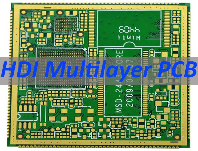
What Is an HDI Multilayer PCB?
An HDI multilayer PCB is a multilayer printed circuit board built with high-density interconnect technology. Compared with a standard multilayer PCB, it usually has finer line width and spacing, smaller vias, higher wiring density, and more complex interlayer connections.
Typical HDI features include:
- Microvias
- Blind vias
- Buried vias
- Laser drilling
- Sequential lamination
- Fine line and spacing
- Smaller pads
- Higher layer count
- Controlled impedance
- Dense BGA or fine-pitch component routing
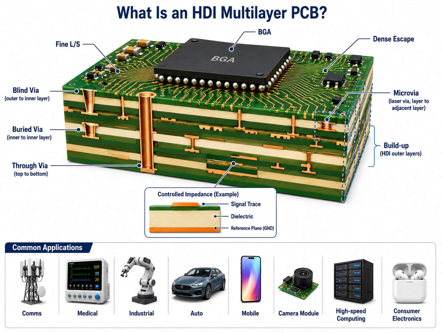
The purpose of HDI is to make the circuit board smaller, denser, faster, and more suitable for modern electronic products. It helps engineers route signals under fine-pitch BGAs, reduce routing congestion, improve signal paths, and support compact mechanical designs.
HDI multilayer PCB is commonly used in communication modules, medical devices, industrial control products, automotive electronics, mobile electronics, camera modules, high-speed computing boards, and compact consumer electronics.
HDI Multilayer PCB Structure and Stackup
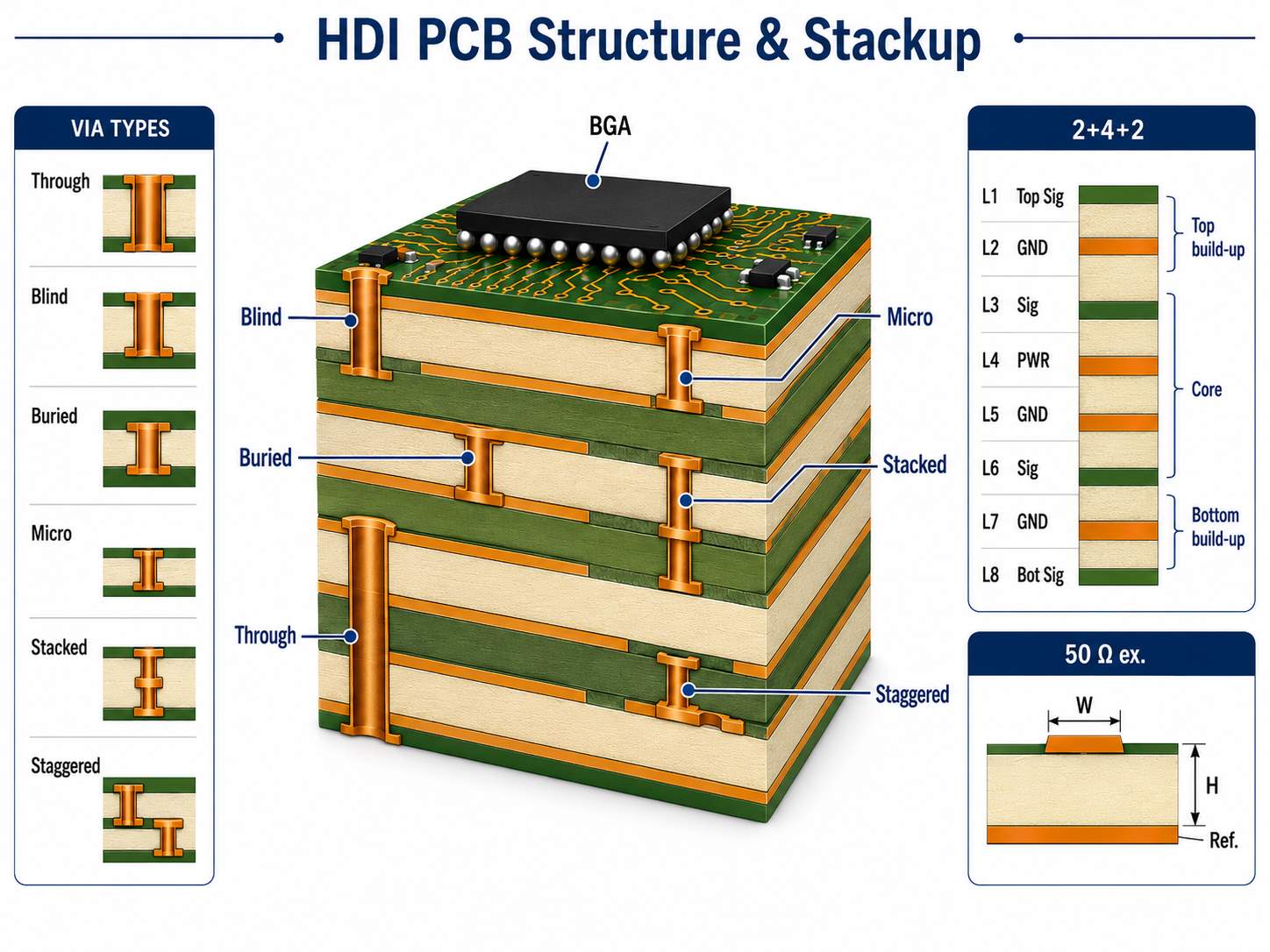
HDI multilayer PCB structure is one of the most important parts of the project. The stackup defines the layer count, dielectric thickness, copper thickness, signal layers, power layers, ground layers, impedance structure, and via connection method.
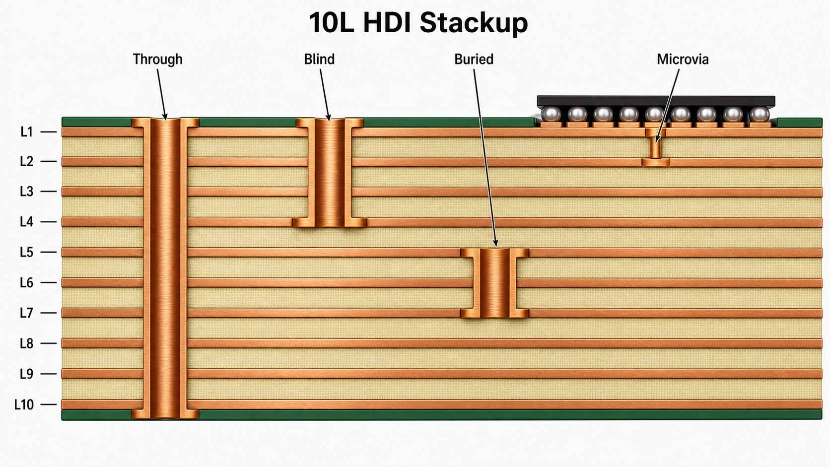
A standard multilayer board may use through holes to connect all layers. An HDI PCB may use several types of vias:
| Via Type | Purpose |
|---|---|
| Through via | Connects from top layer to bottom layer |
| Blind via | Connects an outer layer to one or more inner layers |
| Buried via | Connects inner layers only |
| Microvia | Small laser-drilled via for high-density routing |
| Stacked microvia | Microvias stacked across layers |
| Staggered microvia | Microvias offset between layers |
The stackup must be reviewed before production because HDI boards are sensitive to lamination, drilling, plating, and reliability. A good HDI stackup should support routing density, impedance control, manufacturability, and assembly reliability at the same time.
For example, if the board uses fine-pitch BGA components, the stackup may need microvias to escape signals from the BGA area. If the board also has high-speed signals, impedance must be calculated based on copper thickness, dielectric thickness, reference layers, and trace geometry.
Multilayer HDI PCB vs Standard Multilayer PCB
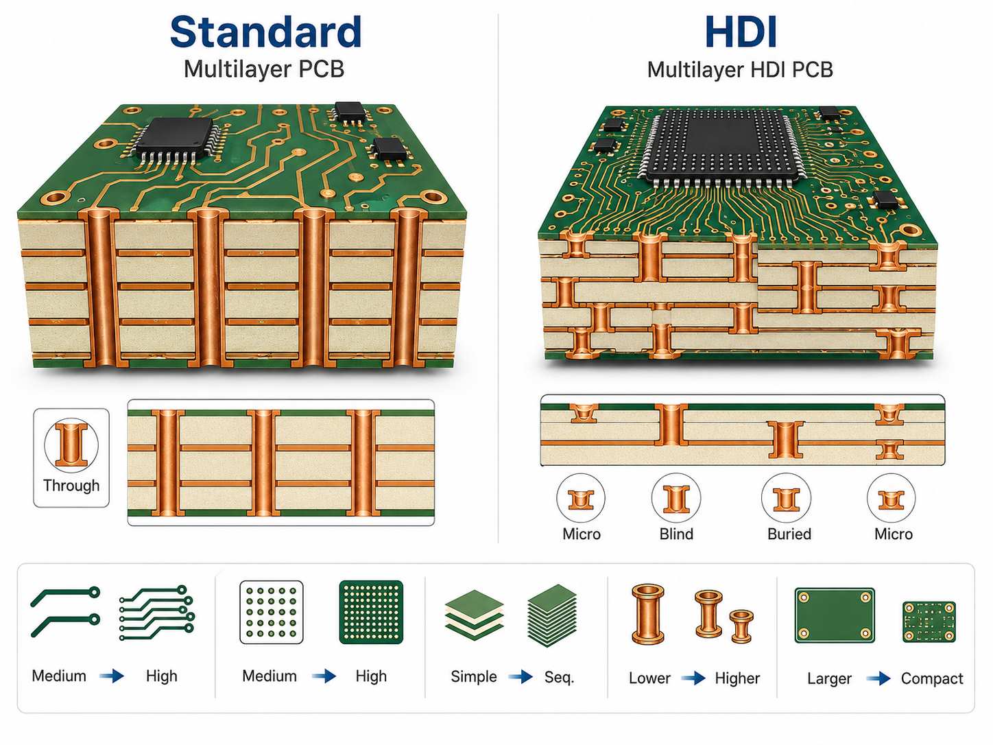
A multilayer HDI PCB is different from a standard multilayer PCB because it uses advanced interconnect methods to increase routing density. Both board types can have many layers, but the difference is how signals move between layers.
| Item | Standard Multilayer PCB | Multilayer HDI PCB |
|---|---|---|
| Via type | Mostly through vias | Microvias, blind vias, buried vias |
| Routing density | Medium to high | Very high |
| Component pitch | Standard to fine pitch | Fine pitch and dense BGA |
| Board size | May be larger | Can be more compact |
| Lamination | Simpler | Often sequential |
| Manufacturing risk | Lower | Higher |
| Cost | Usually lower | Usually higher |
The choice depends on the product. If a standard multi-layer PCB can meet the routing and mechanical requirements, it may be the better choice for cost and simplicity. If the product needs compact size, fine-pitch components, high signal density, or shorter interconnect paths, HDI technology may be necessary.
This is why DFM review matters. Sometimes customers ask for HDI because the design looks dense, but a manufacturability review may show that a standard multilayer solution is still possible. In other cases, HDI is not optional because the component package or product size requires it.
HDI Multilayer Circuit Board PCB Technology
HDI multilayer circuit board PCB technology combines advanced drilling, plating, lamination, and imaging processes. The manufacturing process must control both electrical performance and mechanical reliability.
Key HDI manufacturing technologies include:
- Laser-drilled microvias
- Sequential lamination
- Resin plugging
- Copper plating and via filling
- Fine-line imaging
- Controlled impedance
- X-ray or AOI inspection
- Electrical testing
- Cross-section analysis when required
Resin plugging and plated filling are especially important when the board has via-in-pad or high-density BGA escape routing. If the via is not properly filled and plated flat, soldering defects, voids, poor planarity, or reliability problems may occur during assembly.
For HDI projects, the engineering team should confirm the via structure, pad size, annular ring, aspect ratio, copper thickness, plating requirements, solder mask registration, and surface finish before production.
At EBest Circuit, HDI manufacturing questions are handled before production release. If there is uncertainty in the stackup, via structure, impedance note, or process requirement, our team raises EQs so the customer can confirm the production data before manufacturing starts.
How HDI Multilayer PCB Improves Signal Integrity
HDI multilayer PCB can improve signal integrity by reducing routing length, improving layer transitions, supporting better reference planes, and enabling compact routing around dense components.
Signal integrity can be affected by:
- Long signal paths
- Poor return paths
- Uncontrolled impedance
- Excessive via stubs
- Routing congestion
- Layer transition noise
- Crosstalk
- Poor power-ground structure
HDI can help reduce some of these risks. Microvias create shorter interconnects than long through vias. Better routing density can allow cleaner signal paths. More flexible stackup options can help engineers keep high-speed signals close to solid reference planes.
However, HDI does not automatically solve signal integrity problems. The design still needs proper impedance planning, return path control, differential pair routing, power integrity review, and manufacturing tolerance control.
For high-speed HDI boards, customers should provide impedance requirements clearly. A good impedance note should include the target impedance, trace width and spacing, reference layer, copper thickness, tolerance, and whether an impedance coupon and test report are required.
Microvias, Blind Vias, and Buried Vias in HDI Multilayer PCB
Microvias, blind vias, and buried vias are the core features of many HDI multilayer PCB designs.
A microvia is usually laser-drilled and connects adjacent layers or short layer spans. It helps route signals from fine-pitch components and reduces the need for large through holes. Blind vias connect from an outer layer to an inner layer. Buried vias connect only internal layers and are not visible from the outside.
These via types can make the PCB much denser, but they also increase manufacturing complexity. The manufacturer must control:
- Laser drilling quality
- Via diameter
- Via depth
- Copper plating
- Resin filling
- Lamination sequence
- Registration accuracy
- Reliability under thermal stress
Stacked microvias can save space, but they require careful reliability review. Staggered microvias may improve manufacturability in some cases. Via-in-pad can help with BGA escape routing, but it usually requires resin filling and plated flat processing.
Before production, the HDI via structure should be reviewed by both the customer and manufacturer. A small via decision can affect cost, lead time, yield, and long-term reliability.
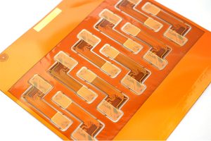
Multilayer Rigid-Flex HDI PCB Applications
Multilayer rigid-flex HDI PCB is used when the product needs high-density routing, flexible connection, and compact mechanical integration at the same time. It is more complex than a standard rigid HDI board because the design must consider both rigid and flexible zones.
Common applications include:
- Medical handheld devices
- Camera and imaging modules
- Aerospace electronics
- Wearable electronics
- Industrial sensors
- Compact communication devices
- Automotive modules
- Portable test instruments
Rigid-flex HDI boards can reduce connectors, save space, improve assembly integration, and increase design flexibility. But they also require careful review of bend radius, flex layer stackup, coverlay, stiffener, copper grain direction, via placement near bend areas, and assembly handling.
For these projects, mechanical drawings are essential. Gerber files alone are not enough. The manufacturer needs to understand which areas bend, which areas stay rigid, where components are mounted, and what the final assembly looks like.
Why Modern Electronics Require HDI Multilayer PCB Technology
Modern electronics require HDI multilayer PCB technology because products are becoming smaller, faster, lighter, and more complex. Components have more pins, smaller pitch, higher signal speed, and stricter mechanical constraints.
HDI technology helps support:
- Smaller product size
- Higher component density
- Fine-pitch BGA routing
- Better signal paths
- Shorter interconnect length
- More compact modules
- More layers in limited space
- Higher function integration
For products such as smartphones, medical devices, industrial controllers, communication modules, camera modules, and high-speed computing boards, HDI may be required to achieve the final design.
But HDI should not be selected only because it sounds advanced. It should be selected when it solves a real routing, mechanical, signal, or product integration problem. A good manufacturer will help review whether HDI is necessary and how to make the structure practical for production.
How to Choose a Multilayer HDI PCB Manufacturer
Choosing a multilayer HDI PCB manufacturer is different from choosing a supplier for a simple 2-layer or 4-layer board. HDI requires tighter engineering communication, stronger process control, and better understanding of stackup, vias, impedance, lamination, and assembly risk.
A reliable multilayer HDI PCB manufacturer should be able to review:
- Layer count and stackup
- HDI buildup type
- Microvia structure
- Blind and buried via structure
- Resin plug and plated flat requirements
- Copper thickness
- Controlled impedance
- Fine line and spacing
- Surface finish
- Solder mask and BGA pad design
- Panelization
- Inspection and testing requirements
- Prototype-to-production consistency
For complex HDI projects, the manufacturer should also ask clear engineering questions before production. This is important because an unclear impedance note, via structure, or stackup assumption can create manufacturing risk.
When evaluating a supplier, do not only ask whether they can “make HDI.” Ask how they review HDI stackups, how they handle microvia reliability, how they confirm impedance, and how they communicate EQs before production release.
HDI Multilayer PCB Manufacturing Case Study
One HDI multilayer PCB project from a Germany-bound industrial electronics customer required a compact, reliable board for a high-density control module. The customer needed more routing density than a standard multilayer PCB could comfortably support, while also keeping the board thin and controlled for assembly.
The project requirements included:
| Project Item | Requirement |
|---|---|
| PCB type | 10L HDI multilayer PCB |
| Material | FR4 Tg170 |
| Copper thickness | Per approved stackup |
| Finished thickness | 1.29221mm +/-10% |
| Solder mask | Green solder mask, white silkscreen |
| Surface finish | ENIG, Au 1u” |
| Via process | Resin plug + plated flat |
| Standard | IPC Class 2 |
| Delivery format | 4up panel per customer panelization |
| Production release | Production data must be confirmed by customer before manufacturing |
For this project, the main risks were stackup accuracy, via filling quality, impedance confirmation, and production data control. Because the board had impedance requirements, EBest Circuit raised EQs before production to confirm the impedance details, stackup expectations, and related manufacturing notes. This step helped avoid assumptions before the board entered fabrication.
The resin plug and plated flat process was also important. For an HDI multilayer PCB with dense routing and possible via-in-pad areas, poor filling or uneven plating can affect soldering, BGA assembly, planarity, and long-term reliability.
The customer also required 4up panel delivery based on their panelization data. That meant the production team needed to follow the customer’s panel file, not create a free panel without confirmation. Before manufacturing, the production data had to be sent back to the customer for approval.
This case shows what customers usually care about in HDI multilayer PCB projects: not only whether the board can be produced, but whether the stackup, via process, impedance, panelization, and confirmation process are controlled clearly before production.
Why Choose EBest Circuit for HDI Multilayer PCB Manufacturing?
EBest Circuit (Best Technology) is a custom PCB and PCBA manufacturer with more than 20 years of experience supporting engineers from prototype to production. For HDI multilayer PCB projects, our value is not only production. It is early engineering review, process matching, and full-chain coordination.
EBest Circuit can support:
- HDI multilayer PCB fabrication
- Stackup and DFM review
- Microvia and via structure review
- Resin plug and plated flat process review
- Controlled impedance review
- Component sourcing
- SMT assembly
- PCBA testing
- Prototype and small-batch production
- Production data confirmation before fabrication
Our team includes PCB/PCBA engineers with long-term manufacturing experience. For complex boards, we can help customers check risk areas before production, including copper thickness, dielectric thickness, impedance, fine line spacing, via structure, panelization, surface finish, and assembly requirements.
EBest Circuit also supports one-stop PCB manufacturing, component sourcing, PCBA assembly, and testing. With our own PCB and PCBA factory, 1,000+ supply chain partners, ISO9001/13485, IATF16949, AS9100D, REACH, RoHS, and UL-related quality systems, we help customers manage both quality and delivery.
If you are developing an HDI multilayer PCB, multilayer rigid-flex HDI PCB, or high-density PCBA project, send your Gerber files, stackup, BOM, drawings, impedance notes, and questions to sales@bestpcbs.com. Our engineering team will help review the manufacturing path before production starts.
FAQs about HDI Multilayer PCB
What is an HDI multilayer PCB?
An HDI multilayer PCB is a high-density interconnect PCB with multiple layers and advanced via structures such as microvias, blind vias, and buried vias. It supports dense routing, fine-pitch components, and compact electronic products.
What is the difference between multilayer PCB and HDI PCB?
A standard multilayer PCB uses multiple copper layers, but it may rely mainly on through vias. An HDI PCB uses microvias, blind vias, buried vias, fine lines, and more advanced stackups to support higher routing density.
Why does HDI multilayer PCB improve signal integrity?
HDI can improve signal integrity by reducing interconnect length, supporting better routing around dense components, reducing via stubs, and helping high-speed signals stay closer to reference planes.
Does HDI multilayer PCB always cost more?
Usually yes. HDI multilayer PCB often costs more than a standard multilayer PCB because it may require laser drilling, sequential lamination, microvia plating, resin filling, and tighter process control.
When should I use HDI multilayer PCB?
Use HDI multilayer PCB when a standard multilayer PCB cannot meet routing density, BGA escape routing, product size, signal integrity, or mechanical integration requirements.
Can EBest Circuit manufacture HDI multilayer PCB?
Yes. EBest Circuit can support HDI multilayer PCB fabrication, DFM review, stackup confirmation, impedance review, component sourcing, SMT assembly, and PCBA testing for prototype and production projects.
If your HDI multilayer PCB project has tight space, impedance requirements, microvias, resin-filled vias, or production data that needs careful review before manufacturing, EBest Circuit (Best Technology) can help you check the stackup, process feasibility, and PCBA path before production starts. Send your Gerber files, stackup, drawings, BOM, or technical questions to sales@bestpcbs.com. Our engineering team will review your project and help you move from prototype to production with clearer technical direction.
You may also like

Tags: hdi multilayer circuit board pcb, hdi multilayer PCB, multilayer hdi pcb manufacturer