





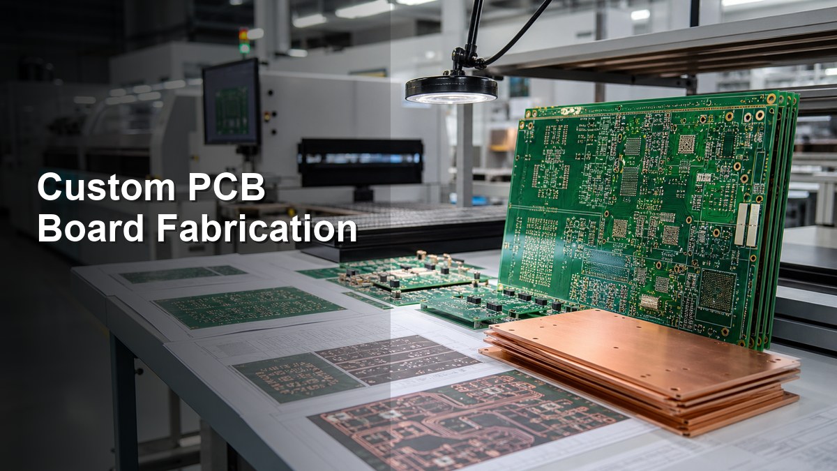
Custom PCB board fabrication is the process of turning production-ready design data into a physical printed circuit board built to a specific stackup, material, copper weight, surface finish, tolerance and inspection requirement. A reliable fabrication order is not defined only by board size or layer count. It depends on clean Gerber or ODB++ data, drill files, material availability, manufacturable design rules, controlled process steps and clear acceptance criteria.
For engineers and buyers, the most useful question is not simply “who can make a custom PCB?” The better question is “what information does the fabricator need to build this board correctly the first time?” This guide explains the file package, material decisions, fabrication steps, inspection checks and supplier questions that matter before RFQ.
What Is Custom PCB Board Fabrication?
Custom PCB board fabrication means manufacturing a bare PCB from a customer-specific design rather than buying a standard off-the-shelf board.
The design may be a simple two-layer FR4 board, a dense multilayer board, an HDI board, a heavy copper power board, a metal-core board, a ceramic substrate, or another application-specific construction. The fabricator prepares production tooling from the supplied data, images the copper layers, drills holes, plates vias, applies solder mask and legend, adds the chosen surface finish, routes or scores the outline, and tests the board before shipment.
A custom board gives the designer control over shape, connector position, layer structure, impedance, copper width, heat path, mounting holes and assembly fit. That control also creates responsibility: unclear design notes, missing drill files or unrealistic tolerances can delay production or create boards that are technically built but not suitable for the final product.
Files Needed Before a PCB Can Be Fabricated
A fabricator can only confirm price, lead time and manufacturability when the production file package describes the board without guessing.
For bare PCB fabrication, send Gerber or ODB++ files, NC drill files, board outline, layer stackup, copper weight, finished thickness, material requirement, solder mask color, legend color, surface finish, impedance notes, controlled-depth drilling notes, special plating requirements and a fabrication drawing if tolerances matter. If the board will later be assembled, include the BOM, centroid file and assembly drawing early so the bare board can support the assembly process.
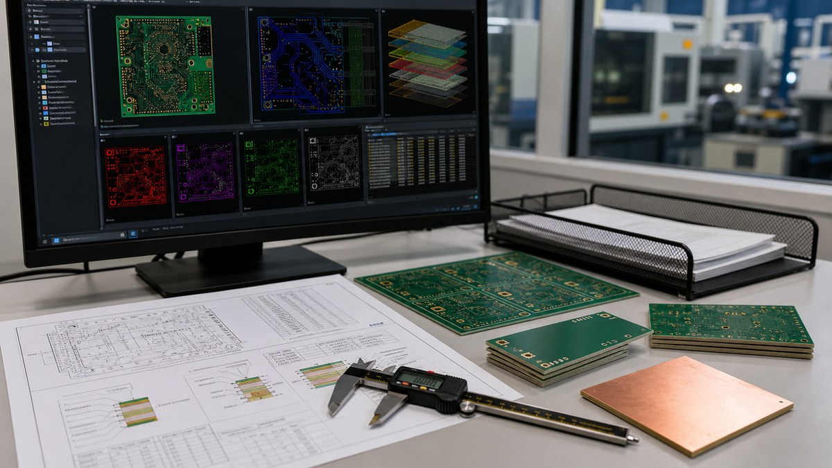
Common file problems include an outline that does not match the mechanical drawing, plated and non-plated holes mixed in one unclear drill file, missing impedance information, no material callout, ambiguous copper weight, or a solder mask opening that conflicts with fine-pitch parts. These problems are easier to fix before fabrication than after panels are released to production.
Material and Stackup Choices That Change Fabrication Risk
Material and stackup decisions control cost, lead time, yield and long-term reliability more than many buyers expect.
Standard FR4 printed circuit board builds are usually easier to quote and schedule than special laminates. However, high Tg FR4, RF material, ceramic substrate, metal-core construction, rigid-flex material and heavy copper boards may be necessary for temperature, power, frequency or mechanical requirements. The right material should be chosen for the operating environment, not only for the lowest unit price.
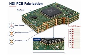
Stackup also matters. Controlled impedance, sequential lamination, buried vias, blind vias, via-in-pad, thin dielectric spacing and unusual finished thickness can all add manufacturing checks. If the design needs high wiring density, compare the layout against realistic HDI PCB process limits before asking for fast delivery.
Typical PCB Fabrication Steps Buyers Should Understand
The fabrication process is a controlled chain of imaging, drilling, plating, finishing and testing steps, so a weak early decision can affect the final board.
| Stage | What Happens | Buyer Check |
| CAM and DFM review | Files are checked for manufacturability, layer alignment, drill data, spacing and special notes. | Confirm all design files match the intended revision. |
| Material preparation | Copper-clad laminate, prepreg, copper foil and special materials are prepared. | Verify material grade, board thickness and copper weight. |
| Inner and outer layer imaging | Copper patterns are transferred and etched according to the design data. | Check fine line and spacing against supplier capability. |
| Drilling and plating | Mechanical or laser holes are drilled, then plated to connect layers. | Review hole size, annular ring and aspect ratio risk. |
| Solder mask and surface finish | Solder mask, legend and finish such as HASL, ENIG, OSP or immersion silver are applied. | Select a finish that fits component type, shelf life and assembly method. |
| Profiling and testing | Boards are routed, V-scored, electrically tested and inspected before packing. | Define acceptance criteria and required reports before production. |
For a broader process reference, Best Technology’s PCB manufacturing page shows how raw material preparation, lamination, drilling, plating, solder mask, testing and packing fit together in a complete bare-board flow.
Design Rules That Should Be Checked Before RFQ
DFM review should focus on the few design limits that can change yield, price or delivery before the buyer approves production.
- Minimum trace width and spacing for the chosen copper weight.
- Minimum mechanical drill, laser drill and finished hole size.
- Annular ring, drill-to-copper clearance and edge-to-copper clearance.
- Aspect ratio for plated through holes and microvia structure for HDI boards.
- Solder mask bridge width for fine-pitch components.
- Controlled impedance stackup, dielectric thickness and copper roughness assumptions.
- Panelization, V-score or routing needs for assembly handling.
- Surface finish compatibility with BGA, fine pitch, wire bonding or storage conditions.
If the project includes SMT, through-hole assembly or turnkey sourcing, bare board fabrication should be planned with PCB assembly support in mind. Pad design, fiducials, panel rails, solder mask openings and test points can make assembly easier or create avoidable rework.
Inspection and Testing Should Be Defined Early
Inspection should match the risk level of the board, not a generic checklist copied from another project.
Typical checks include visual inspection, dimensional measurement, solder mask inspection, electrical open/short testing, impedance coupon testing when specified, microsection review for high-reliability builds, and final packing inspection. For boards used in power electronics, automotive equipment, medical devices, aerospace-related hardware or outdoor products, buyers should define the required standard, report format and acceptance level before quotation.
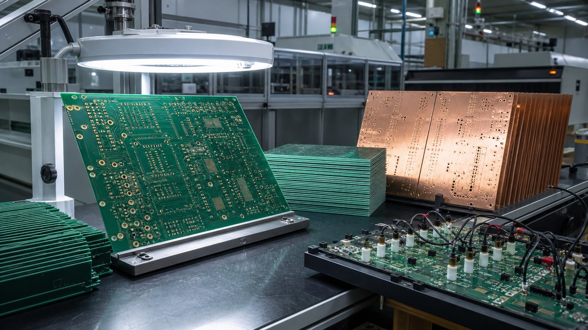
Quality checks are also practical supplier filters. A fabricator that can explain test equipment, inspection points and process records is usually easier to work with than one that only quotes a low price. Best Technology’s PCB test equipment page is a useful internal reference when a buyer wants to understand what inspection capability may be relevant.
Cost and Lead Time Factors in Custom PCB Fabrication
Custom PCB fabrication cost and lead time usually increase when the board needs more controlled process steps or less common material.
Important cost drivers include layer count, panel utilization, board thickness, copper weight, line width and spacing, hole count, smallest drill, blind or buried vias, surface finish, impedance control, special material, testing requirements, quantity and delivery speed. A small board is not always cheap if it requires HDI, heavy copper, tight drilling or special laminate. A larger board may be easier if it uses standard material and relaxed tolerances.
Buyers should ask suppliers to separate tooling, bare board fabrication, assembly, component sourcing, testing and shipping costs when the project includes more than the bare PCB. This prevents a low board price from hiding a high assembly or logistics risk.
Supplier Questions Before You Approve Fabrication
The best RFQ questions help the supplier expose manufacturing risk before the board enters production.
- Are any traces, spaces, holes or annular rings outside standard capability?
- Is the requested material in stock, or does it require special sourcing?
- Does the stackup support the required impedance and finished thickness?
- Is the selected surface finish suitable for the component packages and storage time?
- Are there any panelization issues that could affect assembly or depaneling?
- Which tests are included, and which reports require an extra request?
- What design change would reduce cost, lead time or yield risk?
If the design falls outside standard FR4 or routine multilayer production, a special PCB review can help clarify whether the project needs heavy copper, high-frequency material, metal core, ceramic, rigid-flex or another custom process path.
FAQ
What files are required for custom PCB board fabrication?
Most fabrication orders need Gerber or ODB++ files, NC drill files, board outline, stackup, copper weight, thickness, material, solder mask, legend, surface finish and any special tolerance notes. A fabrication drawing is useful when dimensions, impedance, controlled-depth drilling or acceptance criteria matter.
Is PCB fabrication the same as PCB assembly?
No. PCB fabrication makes the bare printed circuit board. PCB assembly places and solders components onto that board. A turnkey PCBA project needs both steps, plus BOM review, component sourcing, stencil planning, inspection and testing.
What makes a custom PCB harder to fabricate?
HDI microvias, blind or buried vias, heavy copper, tight spacing, unusual thickness, special materials, controlled impedance, fine-pitch solder mask, large panels and strict inspection requirements can all increase fabrication difficulty.
Which surface finish should I choose?
The right finish depends on assembly method, component package, shelf life, flatness and cost. ENIG is often chosen for fine pitch and flatness, HASL can fit less demanding boards, and OSP may fit some cost-sensitive builds. Confirm with the assembler before ordering.
How can I reduce PCB fabrication cost?
Use standard material when possible, improve panel utilization, avoid unnecessary tight tolerances, simplify via structures, keep copper weight realistic, choose a suitable finish and send complete files. Do not remove inspection that protects product reliability.
Can a fabricator fix my PCB design files?
A fabricator can often flag manufacturability issues and suggest changes, but it should not silently change electrical intent. Any change to spacing, pad shape, drill size, stackup or material should be reviewed and approved by the design owner.
When should I request impedance control?
Request impedance control when the board carries high-speed digital, RF, differential pairs, antennas or other signals that depend on trace geometry and dielectric structure. Provide target impedance, tolerance, reference layers and stackup requirements.
Does custom PCB fabrication always take longer than standard PCB orders?
Not always. A custom board with standard FR4, clean files and routine tolerances can move quickly. Lead time increases when the design needs special material, complex stackup, extra testing, unusual finish or unresolved DFM clarification.
Final Thoughts
Custom PCB board fabrication is predictable when the design files, stackup, material choices, process limits and inspection requirements are clear before production. The safest RFQ is not the one with the fewest details. It is the one that lets the supplier identify cost, lead time and yield risk before the first panel is built.
If you are preparing a custom PCB for prototype or production, send your Gerber, drill, stackup, BOM and assembly files to the Best Technology engineering team at sales@bestpcbs.com for fabrication, PCBA and quotation review.
You may also like



Tags: Custom PCB, DFM, pcb fabrication, pcb manufacturing