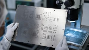
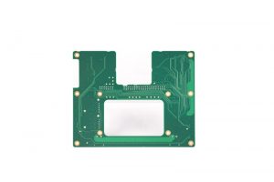
A solder paste stencil is one of the first process tools used in SMT PCB assembly, but it has a direct impact on final soldering quality. It controls solder paste volume, pad coverage, paste release, and solder joint consistency after reflow. A well-designed stencil helps reduce common SMT defects such as solder bridging, insufficient solder, tombstoning, solder balls, BGA open joints, and excessive voiding under exposed pads.
EBest Circuit supports SMT stencil and PCB assembly projects with laser-cut stencils, etched stencils, framed and frameless options, electro-polished apertures, fiducial marks, step-up/down technology, and BGA ball mounting stencils. Our team can review Gerber files, paste layers, BOM, Pick-and-Place files, and assembly requirements before production to help improve solder paste printing stability. For solder paste stencil support or full and partial turnkey PCB assembly, please send your files and requirements to sales@bestpcbs.com.
What Is a Solder Paste Stencil?
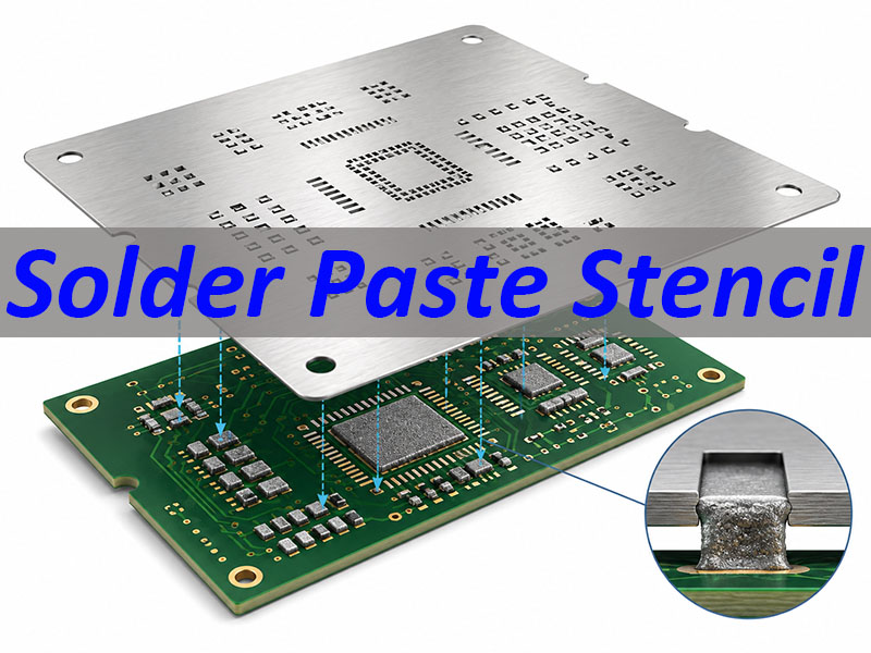
A solder paste stencil is a thin sheet used to print solder paste onto PCB pads before surface mount components are placed. It is usually made from stainless steel and has precise openings called apertures. These apertures match the solder paste layer in the PCB design files.
During printing, the stencil is aligned over the PCB. A squeegee pushes solder paste across the stencil surface. The paste passes through the apertures and lands on the PCB pads. After stencil separation, each pad should have a controlled solder paste deposit.
In simple terms:
A solder paste stencil controls paste volume, paste location, and printing consistency in SMT assembly.
A stencil affects:
- Solder joint volume
- Paste printing accuracy
- Fine-pitch component quality
- BGA and QFN soldering
- LED and connector solder strength
- SMT defect rate
- PCBA production repeatability
For simple PCB prototypes, a standard stencil may be enough. For fine-pitch ICs, BGA packages, QFN exposed pads, 0201 components, connectors, or LED metal core PCB, stencil design needs a more detailed review.
How Does a Solder Paste Stencil Work in SMT PCB Assembly?
A solder paste stencil is used at the solder paste printing stage. This is one of the earliest and most important steps in SMT assembly. If the paste printing result is unstable, later processes such as placement, reflow, AOI, and X-ray inspection will face more risk.
A typical SMT assembly flow includes:
- Material and PCB preparation
- Baking when required
- Solder paste printing
- SPI inspection
- Component placement
- Reflow soldering
- AOI inspection
- X-ray inspection for BGA or hidden joints
- Functional testing
- Cleaning and final packaging
The stencil is mainly used during the solder paste printing step. However, its effect can be seen throughout the whole process.
| SMT Stage | Stencil Impact |
|---|---|
| Paste printing | Controls paste volume |
| SPI | Checks paste quality |
| Placement | Supports stable mounting |
| Reflow | Affects solder joints |
| AOI | Reveals visible defects |
| X-ray | Checks hidden joints |
A good stencil helps solder paste transfer cleanly from the aperture to the pad. A poor stencil may leave paste inside the opening, print too much paste, or cause offset deposits.
In production, engineers often check stencil design when defects repeat on the same pads. If the same IC pins keep bridging, or the same QFN center pad has too much solder, the stencil is usually one of the first items to review.
PCB Stencil vs Solder Paste Stencil: Are They the Same?
In most SMT projects, a PCB stencil and a solder paste stencil refer to the same tool. Both are used to print solder paste onto PCB pads.
The difference is mainly in wording.
| Term | Meaning |
|---|---|
| Solder paste stencil | Most precise term |
| PCB stencil | Common buyer term |
| SMT stencil | Factory process term |
| Solder stencil | Shorter informal term |
| Circuit board stencil | General search term |
If you are ordering a stencil for assembly, “solder paste stencil” is the clearest term. It tells the supplier that the stencil is used for SMT solder paste printing, not for marking, coating, or another process.
For accurate stencil production, the supplier usually needs:
- Gerber files
- Paste layer
- PCB outline
- Fiducial marks
- BOM
- Pick-and-Place file
- Assembly drawing
- Panel drawing, if applicable
The paste layer is important, but it is not always enough. For better PCBA quality, the stencil should be checked together with component packages and assembly requirements.
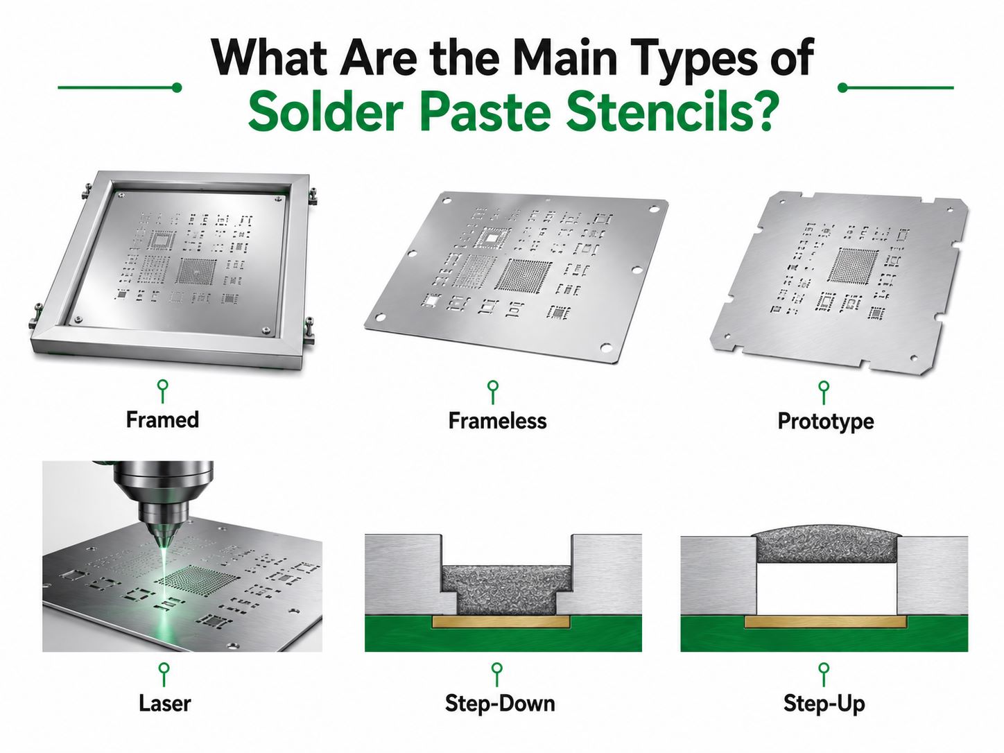
What Are the Main Types of Solder Paste Stencils?
Different PCB assembly projects need different stencil types. A prototype board, a high volume PCB assembly order, and a fine-pitch BGA board may require different stencil choices.
| Stencil Type | Best For | Key Value |
|---|---|---|
| Framed stencil | Mass production | Stable printing |
| Frameless stencil | Low-volume orders | Flexible use |
| Prototype stencil | Samples | Fast setup |
| Laser stencil | Fine-pitch SMT | High accuracy |
| Etched stencil | General use | Cost control |
| Step-down stencil | Mixed components | Local paste control |
| Step-up stencil | Large pads | Extra paste volume |
| BGA ball mounting stencil | BGA repair or mounting | Ball placement |
| PE stencil | Special applications | Lightweight option |
Most SMT stencils today are laser cut because laser cutting offers better aperture accuracy and smoother geometry. Etched stencils are still available for some cost-sensitive or less complex applications.
For higher precision, laser cut stencils may also be electro-polished. Electro-polishing helps smooth the aperture wall and supports better solder paste release. This is especially useful for fine-pitch ICs, QFN pads, small chip components, and dense layouts.
How to Choose the Right Solder Paste Stencil Thickness?
Stencil thickness controls solder paste volume. A thicker stencil prints more paste. A thinner stencil prints less paste. Choosing the right thickness is one of the most important decisions in stencil design.
Common stencil thicknesses include:
| Thickness | Typical Use |
|---|---|
| 0.06 mm | Very fine features |
| 0.08 mm | Miniature SMT |
| 0.10 mm | Fine-pitch ICs |
| 0.12 mm | Standard SMT |
| 0.15 mm | General components |
| 0.20 mm | Larger pads |
| Up to 0.60 mm | Special process |
For most PCB assembly projects, 0.10 mm, 0.12 mm, and 0.15 mm are commonly used. The final choice depends on the smallest component, pad pitch, solder paste type, and required solder volume.
| Component Type | Suggested Thickness | Reason |
|---|---|---|
| 0201 | 0.08–0.10 mm | Less paste |
| 0402 | 0.10–0.12 mm | Stable print |
| 0603 / 0805 | 0.12–0.15 mm | Standard volume |
| Fine-pitch IC | 0.10–0.12 mm | Less bridging |
| QFN / DFN | 0.10–0.12 mm | Better control |
| BGA | 0.10–0.12 mm | Even deposits |
| Connectors | 0.15 mm+ | More solder |
| LED pads | 0.12–0.15 mm | Heat and strength |
| Mixed layout | Step stencil | Local control |
A common problem is mixed component size. One PCB may include a fine-pitch IC and a large connector on the same side. If the whole stencil is too thick, the IC may bridge. If it is too thin, the connector may receive insufficient solder.
There are three common solutions:
- Reduce apertures in fine-pitch areas
- Use window-pane design on large pads
- Use step-up or step-down stencil technology
A good stencil choice should start from the most sensitive component, then adjust aperture design for larger pads.
How Does Aperture Design Affect Solder Paste Printing?
Apertures are the openings in the stencil. They decide where solder paste goes and how much paste reaches the pad.
Stencil thickness controls paste height. Aperture design controls paste area and release behavior. Both must work together.
Important aperture design factors include:
- Aperture size
- Aperture shape
- Opening ratio
- Pad reduction
- Corner radius
- Aperture wall smoothness
- Distance between apertures
- Component package type
| Aperture Design | Used For | Purpose |
|---|---|---|
| 1:1 opening | Normal pads | Standard paste |
| 0.9:1 opening | BGA area | Less excess paste |
| Reduced opening | Fine-pitch IC | Less bridging |
| Home-plate | Chip parts | Less solder balls |
| Window-pane | QFN thermal pad | Less voiding |
| Rounded corners | Small apertures | Better release |
| Segmented opening | Large pads | Even paste |
For standard components, a 1:1 aperture may work well. For BGA areas, a 0.9:1 scale is often used to reduce excess paste and improve solder control.
For QFN or DFN exposed pads, window-pane design is usually better than one large opening. A single large aperture can print too much paste and cause the component to float during reflow. Dividing the opening into smaller windows helps control solder volume.
For LED metal core PCB, stencil design must also consider thermal pads, long strip board shape, and solder joint stability. Long LED strips may need special stencil support, proper panel design, and stable printing fixtures.
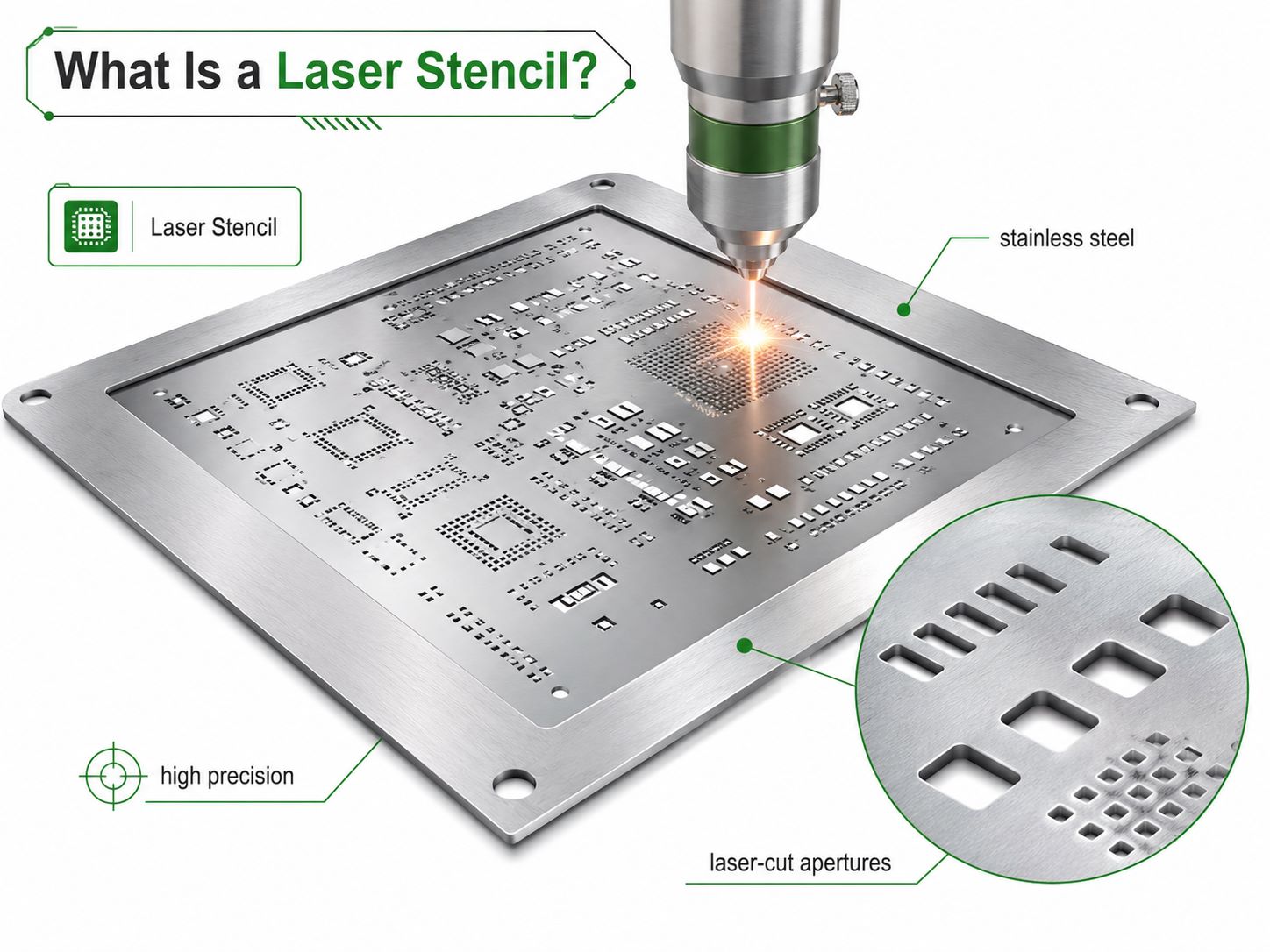
What Is a Laser Stencil?
A laser stencil is a solder paste stencil made by laser cutting. The apertures are cut directly from the design data, usually from Gerber or CAD files.
Laser stencils are widely used because they offer:
- High aperture accuracy
- Clean opening geometry
- Good repeatability
- Fast production
- Fine-pitch support
- Compatibility with electro-polishing
- Stable SMT printing performance
At EBest Circuit, most SMT stencils are laser cut. Etched stencils are also available when the project requirements are suitable.
Laser cut stencils are especially useful for:
- BGA packages
- Fine-pitch ICs
- QFN and DFN packages
- 0201 and 0402 components
- High-density PCB layouts
- Medical electronics
- Communication modules
- Automotive PCBA
- Industrial control boards
For better paste release, laser cut stencils can be electro-polished. Smooth aperture walls help solder paste release more easily, reduce cleaning frequency, and improve SMT printing efficiency.
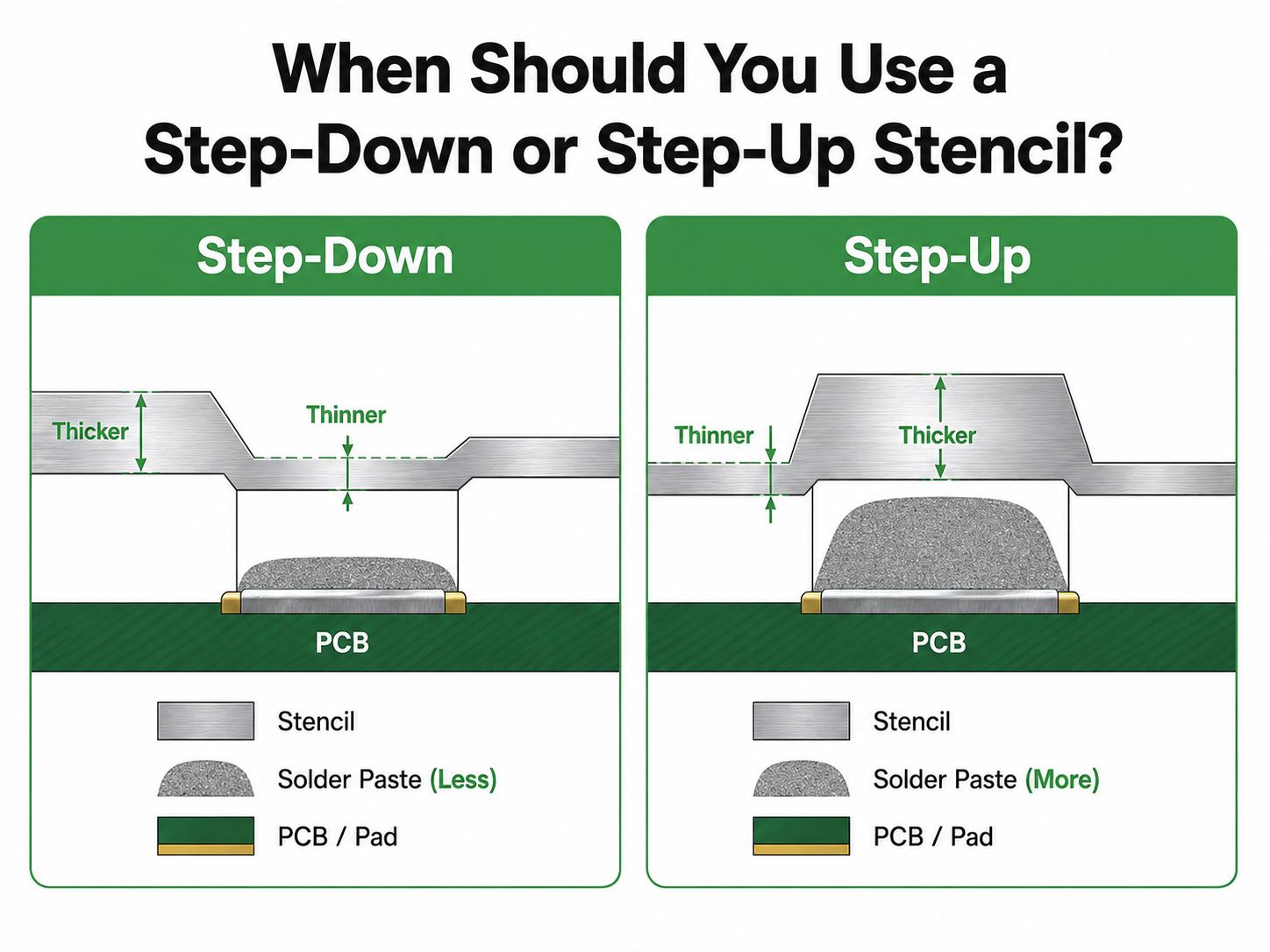
When Should You Use a Step-Down or Step-Up Stencil?
A step-down stencil has selected areas that are thinner than the main stencil. A step-up stencil has selected areas that are thicker than the main stencil.
These designs are used when different components on the same PCB need different solder paste volumes.
| Stencil Design | Function | Typical Use |
|---|---|---|
| Step-down | Less paste locally | Fine-pitch IC |
| Step-up | More paste locally | Connector pad |
| Mixed step | Different paste levels | Complex PCB |
Use a step-down stencil when:
- Fine-pitch ICs are bridging
- Small components need less paste
- QFN areas need tighter paste control
- BGA areas require stable deposits
- Dense layouts have limited spacing
Use a step-up stencil when:
- Connectors need stronger joints
- Large terminals need more solder
- Shielding parts need higher paste volume
- Special pads require extra solder height
Step stencil design should be reviewed carefully. The step edge should not be too close to active apertures. If the step area is too near component pads, the squeegee may not print evenly.
For many boards, aperture modification is enough. Step-up or step-down technology is more useful when aperture changes alone cannot balance solder volume.
Common Solder Paste Stencil Problems and Solutions
Many SMT defects begin at the solder paste printing stage. A good stencil can reduce these issues, but process control is also important.
| Defect | Likely Cause | Solution |
|---|---|---|
| Bridging | Too much paste | Reduce aperture |
| Insufficient solder | Poor release | Clean or adjust stencil |
| Missing paste | Blocked aperture | Clean stencil |
| Offset paste | Bad alignment | Check fiducials |
| Tombstoning | Uneven paste | Balance apertures |
| Solder balls | Excess paste | Use better aperture |
| QFN floating | Large center paste | Use window-pane |
| BGA open | Low paste volume | Check aperture |
| Voiding | Poor pad design | Segment aperture |
| Frequent cleaning | Rough walls | Use polishing |
A stencil problem is more likely when the defect appears repeatedly in the same area. A process problem is more likely when the defect appears randomly across the board.
For example:
- Same IC pins bridge every time: check aperture width.
- Same QFN floats after reflow: check thermal pad opening.
- Random missing paste: check stencil cleaning and paste condition.
- Paste offset on many pads: check alignment and PCB support.
SPI inspection is useful here. It can check solder paste area, volume, height, thickness, short risk, and offset before components are placed. This makes stencil and printing problems easier to catch early.
How Long Can a Solder Paste Stencil Be Used?
A solder paste stencil does not last forever. In regular SMT production, its service life is usually around 50,000 prints. However, this number is not the only standard. The actual usable life depends on stencil tension, printing frequency, aperture wear, cleaning condition, storage time, and whether the stencil can still provide stable solder paste release.
In production, stencil life is usually checked by:
- Printing count
- Frame tension
- Aperture wear
- Paste release quality
- Cleaning result
- Storage time
- Production history
| Check Item | Practical Standard | Why It Matters |
|---|---|---|
| Printing count | Around 50,000 prints | Tracks stencil usage |
| Stencil tension | Scrap if ≤25N | Keeps printing stable |
| Aperture wear | Check visually | Affects paste shape |
| Paste release | Check print result | Affects solder volume |
| Cleaning result | No blocked apertures | Prevents missing paste |
| Storage time | Review after long idle time | Avoids old tooling risk |
| Repeat order gap | Review if no order for 3 years | Confirms stencil reliability |
For framed stencils, tension should be checked before and after use. The measurement should not be taken at only one point. It is better to check the four corners and the center area, because uneven tension can cause local solder paste printing defects.
If the stencil tension becomes weak, the printing count is over the control limit, the apertures are worn, or the stencil has been stored for too long, printing stability may decrease. For repeat PCB orders after a long gap, the old stencil should be inspected before reuse. If it no longer meets the production requirement, making a new stencil is safer than risking unstable SMT printing.
What Files Are Needed to Make a PCB Stencil?
To make a solder paste stencil, the paste layer is the key file. However, for better assembly results, the supplier should review more than one file.
| File | Purpose |
|---|---|
| Gerber | PCB data |
| Paste layer | Aperture source |
| BOM | Package check |
| Pick-and-Place | Position check |
| Assembly drawing | Polarity and side |
| Panel drawing | Production layout |
| Special notes | Process needs |
The required data may come from different file formats, such as Gerber, PCB, CAD, Protel, or other electrical design files.
Direct data input from customer files helps reduce manual conversion errors. It also makes stencil production faster and more accurate.
Before ordering a stencil, confirm:
- Top side or bottom side
- Single stencil or two stencils
- Framed or frameless type
- Stencil thickness
- Fiducial marks
- Step-up or step-down areas
- BGA or QFN requirements
- Long board or LED strip requirement
- Shipping and packaging needs
For PCB assembly projects, it is better to send Gerber, BOM, and Pick-and-Place files together. This helps the engineering team check whether the stencil design matches the actual component layout.
How Does EBest Circuit Support SMT Stencil Projects?
EBest Circuit provides SMT stencil support for prototype PCB assembly, low volume PCB Assembly, and production projects. Most of our SMT stencils are laser cut. Etched stencils are also available for suitable applications.
Our stencil service covers both standard and special requirements.
| Capability | Support |
|---|---|
| Lasercut stencil | Available |
| Etched stencil | Optional |
| Framed stencil | Available |
| Frameless stencil | Available |
| Stainless steel stencil | Standard |
| PE stencil | Optional |
| Electro-polishing | Available |
| Fiducial marks | Custom position |
| Step-up/down stencil | Available |
| BGA ball mounting stencil | Available |
| LED strip PCB stencil | Available |
Our stencil advantages include:
- Fast stencil preparation after file confirmation
- Direct use of customer design files
- Framed and unframed stencil options
- Stainless steel material for stable printing
- Laser cut apertures for high accuracy
- Electro-polished apertures for better paste release
- Smooth opening walls to reduce cleaning frequency
- Tapered aperture walls to support paste transfer
- Fiducial marks based on project needs
- Step-up and step-down options for mixed components
- Careful packaging to protect the stencil during transport
EBest Circuit also supports PCB fabrication and SMT assembly, so stencil review can be linked with the full PCBA process. This is important because stencil quality should not be judged only by the metal sheet. It should be judged by the solder paste printing result and the final assembly quality.
For projects with BGA, QFN, fine-pitch IC, LED metal core PCB, connectors, or long strip boards, our team can review stencil thickness and aperture design before production. This helps reduce common SMT risks and improves process stability.
How to Choose a PCB Stencil Manufacturer for SMT Assembly
Choosing a PCB stencil manufacturer is not only about price. A low-cost stencil may still cause expensive rework if the aperture design, material, or thickness is not suitable.
A reliable stencil supplier should understand both stencil fabrication and SMT assembly.
| Evaluation Point | What to Check |
|---|---|
| File review | Gerber and paste layer |
| Thickness advice | Based on components |
| Aperture design | Fine-pitch support |
| Special process | Step-up/down |
| Surface quality | Smooth release |
| Delivery | Production schedule |
| Packaging | Transport safety |
| Assembly feedback | SPI/AOI/X-ray link |
A good supplier should be able to answer:
- Why is this thickness selected?
- Should the BGA aperture be reduced?
- Does the QFN pad need window-pane design?
- Is step-down technology necessary?
- Is the board suitable for framed or frameless stencil?
- Will long strip PCB need special support?
- Can the stencil fit the SMT printer frame?
If a supplier only cuts the paste layer without checking the assembly situation, the stencil may still be usable, but it may not be optimized.
For complex PCBA projects, it is better to work with a partner who can review PCB, stencil, solder paste printing, placement, reflow, and inspection together.
Solder Paste Stencil Design Checklist
Before stencil production, use this checklist to reduce avoidable issues.
File checklist
- Gerber files are complete
- Paste layer is included
- BOM is available
- Pick-and-Place file is ready
- Assembly drawing is clear
- Panel drawing is confirmed
Design checklist
- Stencil thickness is selected
- Aperture reductions are reviewed
- BGA areas are checked
- QFN exposed pads are segmented
- Fine-pitch ICs are reviewed
- LED thermal pads are checked
- Connector pads are reviewed
Production checklist
- Framed or frameless type is confirmed
- Fiducial marks are included
- Step areas are defined
- Printer frame size is suitable
- PCB support method is clear
- SPI inspection is planned
- Packaging method is confirmed
Risk checklist
- Mixed components on one side
- Small 0201 or 0402 parts
- Fine-pitch ICs
- Large exposed pads
- Long strip LED boards
- Heavy connectors
- Double-sided SMT
- Old stencil reuse
This checklist is useful for both prototype and batch production. It helps buyers and engineers discuss stencil details before defects appear on the SMT line.
FAQs About Solder Paste Stencil
How long can a solder paste stencil be used?
A solder paste stencil can usually be used for about 50,000 prints in regular SMT production. Its actual life depends on stencil tension, print count, aperture wear, cleaning quality, and storage condition.
When should an SMT stencil be scrapped?
An SMT stencil should be scrapped if the measured tension is ≤25N, if the print count exceeds 50,000 cycles, or if it has not been used for a customer order for around 3 years. In these cases, the stencil may no longer provide stable solder paste printing.
How should stencil tension be checked?
Stencil tension should be checked before and after use. The measurement should cover the four corners and the center area, not just one point, because uneven tension can cause local printing defects.
What solder paste printing problems can SPI detect?
SPI can detect solder paste volume, area, thickness, height, depth, offset, and short-circuit risk. It helps catch printing issues such as missing paste, offset paste, solder bridging, insufficient solder, and paste peaks before component placement.
What are common solder paste stencil thicknesses?
Common stencil thicknesses include 0.06mm, 0.08mm, 0.10mm, 0.12mm, 0.15mm, and 0.20mm. For many SMT PCB assembly projects, 0.10mm, 0.12mm, and 0.15mm are frequently used, while special designs may require thinner, thicker, or step-up/down stencils.
On the whole, a solder paste stencil is a key process tool in SMT PCB assembly. It controls solder paste volume, printing accuracy, aperture release, and the first condition for good solder joints.
A suitable stencil should match the PCB design, component package, paste type, production volume, and inspection requirements. For simple boards, a standard laser stencil may be enough. For fine-pitch ICs, BGAs, QFNs, connectors, LED metal core PCB, or mixed component layouts, stencil thickness and aperture design should be reviewed carefully.
EBest Circuit provides solder paste stencil support together with PCB fabrication and PCB assembly services. We support laser cut stencils, etched stencils, framed and frameless stencils, electro-polished apertures, fiducial marks, step-up/down technology, BGA ball mounting stencils, and stencil solutions for long strip LED metal core PCB.
If your project requires a solder paste stencil or complete SMT PCB assembly, you can send your Gerber files, BOM, Pick-and-Place file, and assembly requirements to sales@bestpcbs.com. Our engineering team can help review the stencil design before production and support your project from prototype to batch assembly.