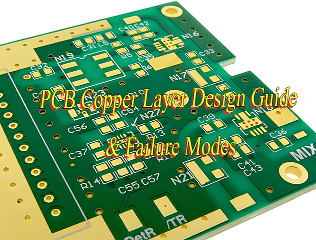
PCB antenna design is not only an RF design topic. It also affects PCB manufacturing, stack-up control, material selection, copper clearance, SMT assembly, enclosure integration, and final product testing.
A good antenna layout can still fail if the manufacturing files are changed incorrectly. Common risks include:
- antenna trace shape modified
- ground plane added under the antenna
- keep-out area filled with copper
- PCB material changed after validation
- stack-up not controlled
- matching components assembled incorrectly
- metal parts placed too close to the antenna
- enclosure changed after RF testing
This article focuses on the manufacturing side of PCB antenna design. It explains what engineers and buyers should check before PCB fabrication and PCBA assembly.
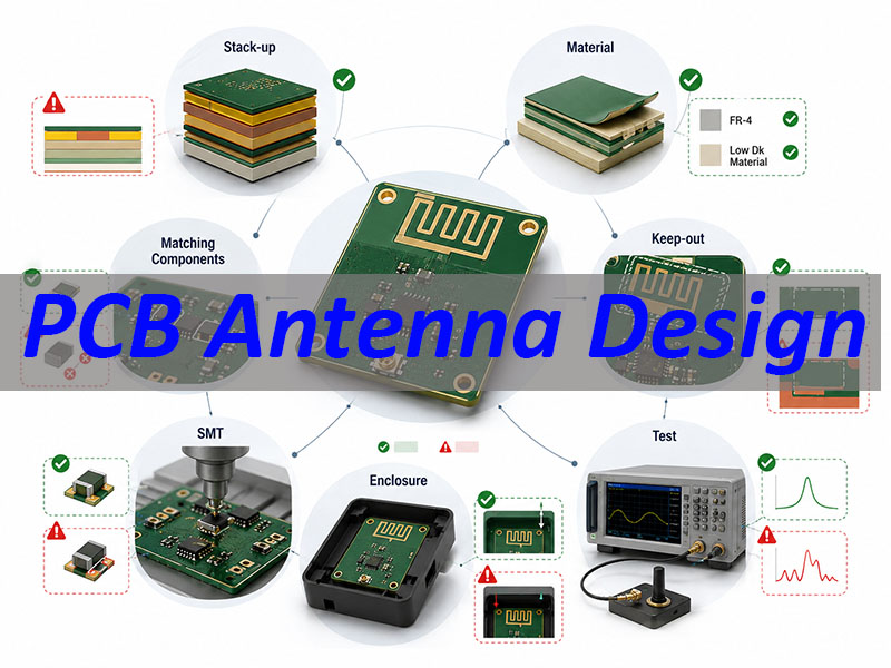
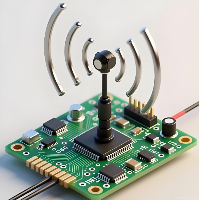
What Is PCB Antenna Design?
PCB antenna design means creating or integrating an antenna structure on a printed circuit board. The antenna may be made from copper traces, a loop coil, a chip antenna layout, or a flexible antenna circuit.
In many wireless products, the antenna is no longer a separate metal part. It becomes part of the PCB system.
Common examples include:
- PCB trace antenna for Bluetooth or Wi-Fi
- PCB loop antenna for NFC or RFID
- chip antenna layout for compact wireless devices
- FPC antenna for wearables or small enclosures
- rigid-flex antenna structure for compact medical or IoT products
A PCB antenna should not be treated as a normal signal trace. It is part of the RF path. Its performance may change when the board outline, material, copper area, stack-up, enclosure, or nearby components change.
For manufacturing, the key point is simple:
Once the antenna is validated, the antenna area should be treated as a controlled RF area.
Why Does Frequency Decide Antenna Size?
Frequency is the first factor that affects PCB antenna size. Lower frequencies have longer wavelengths, so they usually need larger antenna structures. Higher frequencies allow smaller antennas, but they are more sensitive to layout changes.
The basic wavelength formula is:
λ = c / f
Where:
- λ = wavelength
- c = speed of light, about 3 × 10⁸ m/s
- f = frequency
A common antenna reference is quarter wavelength:
L ≈ λ / 4
This does not mean every PCB antenna is exactly one-quarter wavelength. It is only a starting reference. The final length depends on PCB material, effective dielectric constant, ground plane, trace shape, enclosure, and tuning.
| Frequency | Wavelength | 1/4 Wave | Typical Use |
|---|---|---|---|
| 13.56 MHz | 22.1 m | 5.53 m | NFC |
| 433 MHz | 69.3 cm | 17.3 cm | Sensor |
| 915 MHz | 32.8 cm | 8.2 cm | RFID / IoT |
| 2.4 GHz | 12.5 cm | 3.1 cm | BLE / Wi-Fi |
These are free-space reference values. The real PCB antenna size is usually adjusted through trace geometry, ground reference, matching network, and RF testing.
This is why the target frequency must be confirmed before PCB layout and manufacturing review.
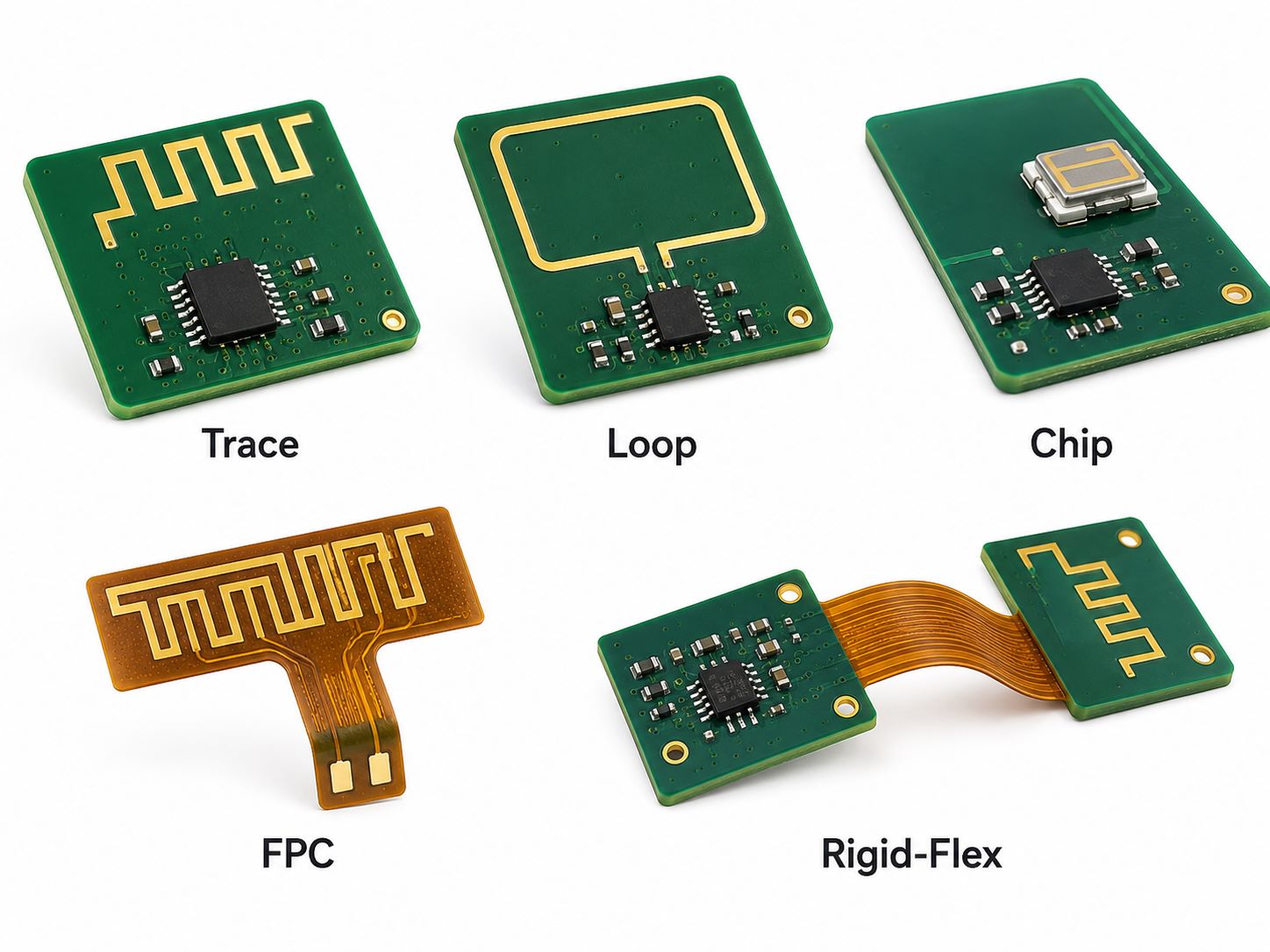
Which PCB Antenna Types Affect Manufacturing?
Not all PCB antennas create the same manufacturing risk. Some are mainly controlled by copper geometry. Some depend more on component placement, soldering, or mechanical bonding.
| Antenna Type | Main Manufacturing Focus | Typical Risk |
|---|---|---|
| PCB trace antenna | Copper geometry | Shape change |
| PCB loop antenna | Coil width / spacing | Inductance shift |
| Chip antenna | Placement / keep-out | Ground error |
| FPC antenna | Bonding / bending | Mechanical stress |
| Rigid-flex antenna | Transition area | Reliability risk |
Each type should be reviewed differently.
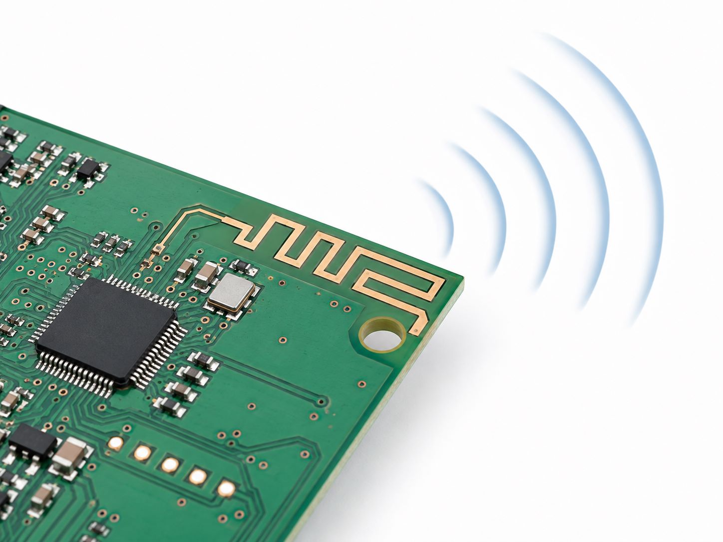
PCB trace antenna
- antenna is made by PCB copper
- copper shape must not be changed casually
- nearby ground and copper must be controlled
- board edge and enclosure affect performance
PCB loop antenna
- often used in NFC or RFID products
- coil size, turns, trace width, and spacing matter
- nearby metal may reduce coupling
- resonance depends on inductance and capacitance
Chip antenna
- antenna is a mounted component
- datasheet layout should be followed closely
- ground clearance and keep-out area are critical
- matching network is usually required
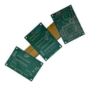
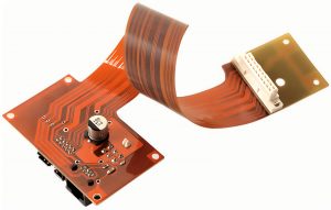
FPC or rigid-flex antenna
- useful when main PCB space is limited
- mechanical placement affects RF performance
- bending, bonding, and connector stress should be reviewed
The antenna type should be confirmed early because it affects PCB layout, material, process, and assembly method.
How Should PCB Trace Antenna Layout Be Protected?
PCB trace antenna layout is very sensitive to changes. A small copper modification may shift the resonant frequency or reduce signal range.
Before fabrication, the antenna area should be locked or clearly marked.
Key items to protect include:
- antenna copper shape
- antenna length
- trace width
- board edge position
- RF feed line
- matching component footprint
- ground clearance
- copper keep-out area
| Layout Item | Manufacturing Rule |
|---|---|
| Antenna shape | Do not modify |
| Board edge | Keep fixed |
| Feed line | Follow impedance |
| Matching area | Keep close |
| Copper nearby | Keep out |
| Ground nearby | Follow RF layout |
The RF feed line is often designed for 50 Ω impedance. Its width depends on the stack-up, dielectric thickness, dielectric constant, and copper thickness.
The guided wavelength inside a PCB is shorter than free-space wavelength:
λg ≈ λ0 / √εeff
Where:
- λg = guided wavelength
- λ0 = free-space wavelength
- εeff = effective dielectric constant
This explains why the same antenna shape may behave differently if the PCB stack-up or material changes.
For manufacturing, the safest rule is:
Do not optimize, fill copper, move traces, or change board outline around the antenna area without RF approval.
Why Are Ground Plane and Keep-Out Areas Critical?
Ground plane and keep-out area are two of the most common causes of antenna problems. The antenna needs a controlled electromagnetic environment. Extra copper, ground, metal, or components can detune the antenna.
A keep-out area is a protected region around the antenna. It is not a free layout area.
Common keep-out restrictions include:
- no copper pour
- no ground plane
- no high-speed traces
- no metal parts
- no large components
- no battery overlap
- no shield cover
- no unapproved test points
| Nearby Object | Possible Effect |
|---|---|
| Ground plane | Detuning |
| Copper pour | Efficiency loss |
| Battery | Absorption |
| Metal housing | Signal loss |
| Shield cover | Pattern shift |
| High-speed trace | Noise coupling |
For chip antennas, the supplier’s datasheet normally defines the keep-out area. For PCB trace antennas, the keep-out rule usually comes from the RF reference layout.
For loop antennas used in NFC or RFID, metal under the coil may reduce magnetic coupling. If the antenna is close to metal or battery structures, ferrite material may be required.
The keep-out area should be shown clearly in the Gerber file, assembly drawing, or engineering notes. It should remain controlled from prototype to mass production.
How Do PCB Material and Stack-Up Changes Affect Antenna Performance?
PCB material and stack-up can affect antenna impedance, resonance, and repeatability. This becomes more important as frequency increases.
Important material-related parameters include:
- Dk: dielectric constant
- Df: loss tangent
- dielectric thickness
- copper thickness
- layer stack-up
- solder mask
- surface finish
- impedance target
| Factor | Possible Impact |
|---|---|
| Dk change | Frequency shift |
| Df change | Higher loss |
| Thickness change | Impedance shift |
| Copper change | Geometry change |
| Stack-up change | Feed mismatch |
| Solder mask change | Small RF shift |
For many standard wireless products, FR4 can be used. But once the antenna has been validated, the FR4 grade and stack-up should not be changed casually.
For higher-frequency or performance-sensitive products, RF laminates may be required for lower loss and better dielectric stability.
Loop antennas and matching networks are often related to LC resonance:
f0 = 1 / (2π√LC)
Where:
- f0 = resonant frequency
- L = inductance
- C = capacitance
If material, copper spacing, coil geometry, or nearby copper changes, the effective L or C may also change. This can shift the resonance away from the target frequency.
Material control is not only a purchasing issue. It is part of RF performance control.
What Should Be Checked Before Antenna PCB Fabrication?
Before antenna PCB fabrication, the supplier should review both normal manufacturability and RF-sensitive areas.
The goal is to prevent silent changes during PCB production.
| File / Item | Why It Matters |
|---|---|
| Gerber | Antenna copper |
| Stack-up | RF feed line |
| Material | Dk / Df control |
| Impedance data | 50 Ω path |
| Antenna notes | Keep-out control |
| BOM | Matching parts |
| PNP file | SMT placement |
| Test plan | Validation scope |
Before release, the following questions should be checked:
- Is the antenna type confirmed?
- Is the target frequency confirmed?
- Is the antenna copper locked?
- Is the keep-out area marked?
- Is the stack-up fixed?
- Is the material specified?
- Is the RF feed impedance defined?
- Are matching components included?
- Are nearby copper areas controlled?
- Is the enclosure already considered?
These checks reduce the risk of building a PCB that is correct electrically but unstable in RF performance.
If any antenna-related item changes after RF validation, the antenna may need to be retested.
What Can Affect Antenna Performance During PCBA Assembly?
Antenna performance may change after PCBA assembly. Components, soldering, shielding, batteries, cables, displays, and enclosure parts can all affect the antenna environment.
Important PCBA checks include:
- matching component values
- matching component placement
- chip antenna orientation
- solder joint quality
- shield cover position
- battery location
- cable routing
- connector position
- enclosure material
- final test condition
| Assembly Item | Risk |
|---|---|
| Wrong matching part | Poor tuning |
| Chip antenna shift | Range loss |
| Shield cover | Detuning |
| Battery position | Absorption |
| Cable routing | Coupling |
| Metal screw | Signal loss |
A bare antenna PCB may perform differently from the final assembled product. This is why RF validation should be done after the product is assembled in its real mechanical environment.
For production, the assembly team should not move RF components or change the matching area without approval.
The RF design team controls tuning and performance validation. The PCBA manufacturer controls placement accuracy, soldering quality, process consistency, and traceability.
How Can EBest Circuit Support Antenna PCB and PCBA Manufacturing?
EBest Circuit (Best Technology) supports antenna PCB and antenna PCBA projects from the manufacturing and assembly side.
Our support focuses on making antenna-related boards manufacturable, repeatable, and assembly-ready.
| Support Area | Value |
|---|---|
| DFM review | Risk reduction |
| PCB fabrication | Stable build |
| Material review | RF consistency |
| Stack-up review | Impedance support |
| Controlled impedance | RF feed path |
| Flex / rigid-flex | Compact devices |
| SMT assembly | PCBA delivery |
| BOM review | Part accuracy |
| Inspection | Process control |
| Traceability | Batch control |
We can support:
- rigid PCB manufacturing
- flex PCB manufacturing
- rigid-flex PCB manufacturing
- antenna PCB DFM review
- stack-up and material discussion
- controlled impedance manufacturing
- fine-line PCB fabrication
- SMT assembly
- customer-supplied parts handling
- inspection and test cooperation
For antenna PCBA projects, we help protect the antenna keep-out area, follow approved stack-up, assemble RF matching components, and support customer-defined tests.
It is also important to define the boundary clearly.
EBest Circuit can support PCB manufacturing, PCBA assembly, DFM review, material and stack-up review, controlled impedance, and test cooperation. Full antenna simulation, RF tuning, S-parameter optimization, wireless range guarantee, and product-level RF certification should be handled by the customer’s RF engineering team or antenna design partner.
This cooperation model keeps responsibility clear and reduces production risk.
FAQs About PCB Antenna Design
What is PCB antenna design?
PCB antenna design is the process of creating or integrating an antenna structure on a printed circuit board. It may use copper traces, loop coils, chip antenna layouts, or flexible antenna circuits.
What is a PCB trace antenna?
A PCB trace antenna is an antenna made from PCB copper. It is common in Bluetooth, Wi-Fi, IoT, and sub-GHz wireless products.
What is a PCB loop antenna?
A PCB loop antenna is a coil-shaped PCB antenna. It is commonly used in NFC, RFID, and near-field communication products.
Why does frequency affect antenna size?
Frequency affects wavelength. Lower frequency means longer wavelength, so the antenna usually needs more space or a meandered trace structure.
What is an antenna keep-out area?
An antenna keep-out area is a protected zone around the antenna. Copper, ground, metal parts, and components should usually be kept away from this area.
Why does PCB material affect antenna performance?
PCB material affects dielectric constant, loss, impedance, and resonance. A material or stack-up change may shift antenna performance.
Can FR4 be used for PCB antenna design?
Yes. FR4 can be used for many standard wireless products. For validated antenna designs, the material grade and stack-up should remain controlled.
What is antenna matching?
Antenna matching adjusts the RF path so energy transfers efficiently between the RF circuit and the antenna. It often uses capacitors and inductors near the antenna feed.
What files are needed for antenna PCB quotation?
Useful files include Gerber, stack-up, material requirement, impedance data, BOM, pick-and-place file, antenna notes, test plan, and quantity.
Can EBest Circuit design the antenna?
EBest Circuit can support PCB manufacturing, DFM review, material and stack-up discussion, controlled impedance, PCBA assembly, and test cooperation. Full antenna simulation and RF tuning should be handled by the customer’s RF engineer or antenna design partner.
In summary, PCB antenna design must be reviewed carefully before manufacturing. Frequency, antenna copper, ground plane, keep-out area, PCB material, stack-up, RF feed line, matching components, PCBA assembly, and enclosure structure can all affect final wireless performance.
For buyers, the best approach is to keep responsibility clear. The RF engineer should design and validate antenna performance. The PCB and PCBA manufacturing partner should control manufacturability, material consistency, antenna area protection, SMT assembly, inspection, and repeatable production.
EBest Circuit (Best Technology) supports antenna PCB and antenna PCBA manufacturing with PCB fabrication, flex and rigid-flex PCB manufacturing, controlled impedance support, DFM review, SMT assembly, material handling, and test cooperation.
For manufacturing review, please send Gerber files, BOM, pick-and-place file, stack-up requirements, antenna notes, impedance data, and test requirements to sales@bestpcbs.com.