

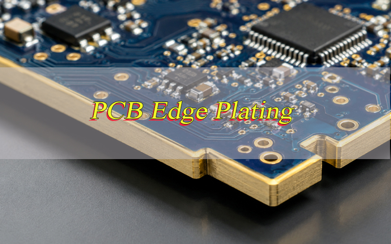
PCB edge plating is used when the edge of a PCB must provide grounding, EMC shielding, side contact, solderable connection or mechanical protection. Unlike normal board routing, the board edge becomes a functional conductive area, so it must be planned before fabrication.
This guide explains edge plating in PCB manufacturing, including process flow, thickness, copper overlap, pullback, solder mask rules, Gerber definition, surface finish, cost, defects and inspection. It helps engineers and buyers reduce design risks before prototype or mass production.
What Is Edge Plating in PCB Manufacturing?
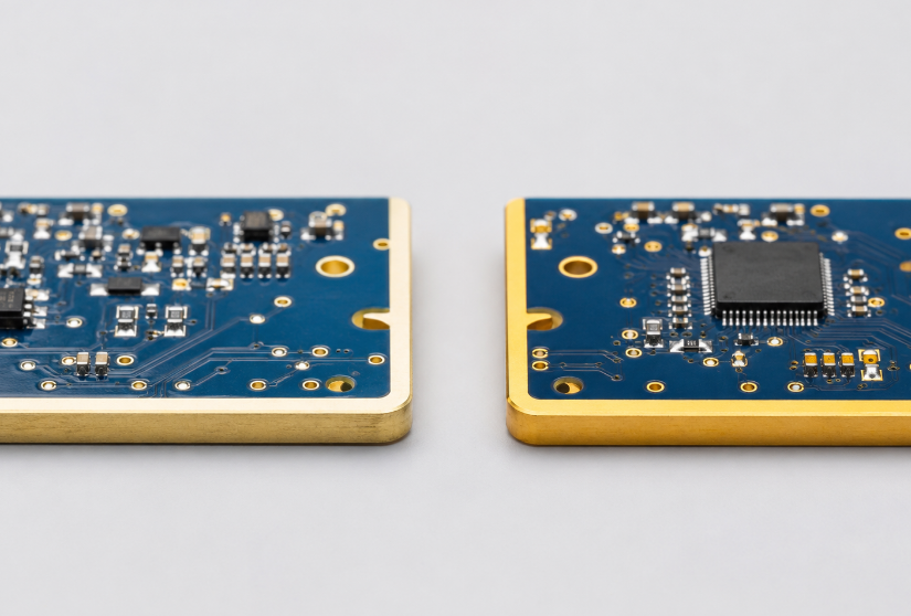
PCB edge plating is a process that deposits copper and surface finish onto the side wall of a PCB. It turns the board edge into a conductive metalized surface connected to selected copper layers.
During PCB edge plating, the routed board edge is exposed before copper deposition. Copper is then built on the vertical side wall. This plated area can connect top copper, bottom copper and internal ground layers when the design is prepared correctly.
The key point is clear: edge plating must be defined before fabrication. Copper overlap, solder mask opening, routing sequence and fabrication notes all affect the final plating quality.
Why Use PCB Edge Plating on a PCB?
PCB edge plating is used when the board edge has an electrical or mechanical function. The main purposes are EMC shielding, grounding, side contact, solderable connection and edge protection.
Main benefits include:
- Improved EMC shielding by connecting the board perimeter to ground.
- Lower grounding impedance for RF, high-speed and shielded circuits.
- Better side contact with metal housings, grounding clips or frames.
- Compact module connection where the edge works as part of the interface.
- Stronger exposed edges compared with bare routed laminate.
For RF modules, wireless products, industrial controllers and shielded electronics, plated edges help improve grounding stability and assembly reliability.
Where Is PCB Edge Plating Commonly Used?
PCB edge plating is commonly used in products that need edge grounding, shielding continuity, side-wall soldering or conductive contact with metal parts. It is most useful when limited board space makes normal pads or connectors difficult.
Common applications include:
- RF and microwave PCB for perimeter grounding.
- WiFi, Bluetooth, GPS and IoT modules for compact wireless assembly.
- EMC shielding PCB connected to metal covers or housings.
- Industrial control PCB used in vibration or harsh environments.
- Medical electronic PCB requiring stable grounding.
- Module carrier boards where edge contact improves assembly density.
PCB round edge plating can also be used, but curved plated edges need better routing control, wider design review and early panel planning.
PCB Side Plating vs Edge Plating: Are They the Same?
PCB side plating and edge plating usually refer to the same process: plating the vertical side wall of the PCB with copper and surface finish. Many manufacturers use both terms in fabrication communication.
The difference is mostly wording. “Edge plating” highlights the plated board outline, while “side plating” highlights the plated vertical wall. For production, the exact drawing is more important than the term.
| Term | Meaning | Use Case |
|---|---|---|
| Edge plating | Conductive plated board edge | Grounding, shielding, edge contact |
| Side plating | Plated vertical side wall | Same process in most factories |
| Plated contour | Plated routed profile | Fabrication drawing notes |
| Metalized edge | Conductive side-wall finish | Engineering communication |
The safest rule is: mark the exact plated area in Gerber files and fabrication notes instead of relying only on wording.
Castellation vs Edge Plating PCB: What Is the Difference?
Castellation and edge plating are related, but they are not the same. Castellation means plated half-holes on the PCB edge, while edge plating means metalizing a routed edge or side wall.
Castellated holes are mainly used for soldering a small module onto a main PCB. A plated edge is mainly used for grounding, shielding, side contact or enclosure connection.
| Item | Castellation | Edge Plating |
|---|---|---|
| Structure | Plated half-holes | Plated side wall |
| Main purpose | Module soldering | Grounding or shielding |
| Shape | Repeated half-hole pads | Continuous or partial edge |
| Risk | Burrs, weak half-hole plating | Shorts, gaps, peeling |
| Assembly role | Board-to-board soldering | Edge contact or shielding |
Castellation and edge plating can appear in the same PCB project, but castellation does not replace edge plating.
What Is the Edge Plating Process of PCB?
The edge plating process of PCB metalizes the routed side wall of the board. It creates conductive copper coverage on the PCB edge for grounding, EMC shielding, side contact or solderable connection.
Step 1: Review the Gerber files
The manufacturer checks the Gerber files, mechanical layer and fabrication notes. The files must show which edge needs plating, where plating starts and stops, and which net it connects to.
Step 2: Check copper overlap and pullback
Connected copper should extend to the plated edge. A common rule is at least 0.5 mm copper overlap. Unrelated copper, power planes and signal traces should be pulled back to prevent shorts.
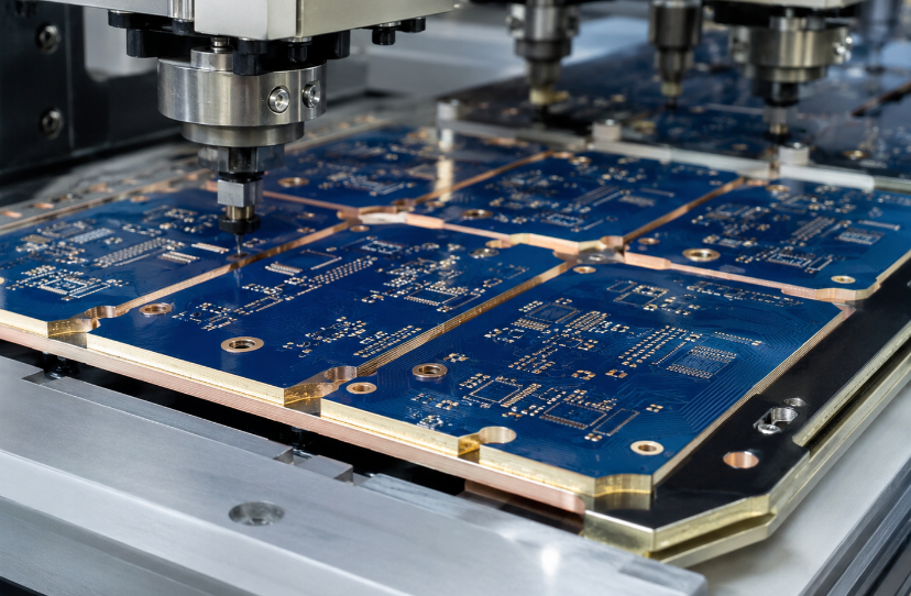
Step 3: Route the edge before plating
The plated edge is routed or milled before copper plating. This exposes the side wall so copper can deposit on it. If the board is routed only after plating, the edge will remain bare.
Step 4: Clean the side wall
The exposed edge is cleaned to remove resin dust, glass fiber debris, burrs and oxidation. Poor cleaning can cause peeling, voids or incomplete edge coverage.
Step 5: Deposit electroless copper
A thin electroless copper layer is applied to the side wall. This creates a conductive seed layer for later electroplating and helps copper cover the non-conductive laminate edge.
Step 6: Build copper thickness
Electrolytic copper plating builds the required edge copper thickness. For common grounding and shielding use, 18–35 μm copper is often used. Higher contact strength may require thicker copper.
Step 7: Control solder mask opening
Solder mask should expose the functional plated edge and cover non-functional copper. A common solder mask pullback range is 0.5–1.25 mm near the plated edge.
Step 8: Apply surface finish
The plated edge receives the required finish. ENIG is suitable for most grounding and shielding designs. Hard gold is better for repeated contact or wear-resistant edges.
Step 9: Final routing and separation
The PCB is separated from the panel after plating and finish. If support tabs are needed, their positions should be confirmed early because they may leave small non-plated areas.
Step 10: Inspect the plated edge
The finished edge is checked for coverage, adhesion, burrs, scratches, exposed laminate, thickness and electrical continuity. Critical boards may need XRF, cross-section and adhesion testing.
In short, the PCB edge plating process depends on clear file definition, pre-plating routing, proper copper overlap, clean side-wall preparation, suitable finish and final inspection.
What Thickness for PCB Edge Plating?
PCB edge plating thickness depends on board function, copper weight, surface finish and reliability requirements. For most projects, the priority is continuous side-wall coverage and strong adhesion, not only a single thickness number.
Common production references include:
| Parameter | Common Range |
|---|---|
| Edge copper thickness | 18–35 μm |
| Higher reliability copper | 35–70 μm |
| ENIG nickel | 3–6 μm |
| ENIG gold | 0.05–0.1 μm |
| Hard gold | 0.5–1.5 μm |
| Copper overlap | ≥0.5 mm |
| Solder mask pullback | 0.5–1.25 mm |
For normal grounding and shielding, 35 μm copper is a practical starting point. For repeated contact or wear areas, hard gold and thicker plating may be required.
These values are common engineering references. Final acceptance should follow customer drawings, IPC class requirements and the manufacturer’s approved capability.
What Are the Minimum Copper Overlap and Pullback Rules for PCB Edge Plating?
Copper overlap and pullback rules prevent open circuits, weak plating and shorts to internal layers. The copper that must connect to the plated edge should reach the board side wall, while unrelated copper must stay away.
Recommended starting rules include:
- Minimum copper overlap: at least 0.5 mm into the plated edge area.
- Connected copper width: at least 0.3 mm where the layer joins the edge.
- Non-connected copper pullback: at least 0.8 mm from the plated outline.
- Different-net clearance: at least 0.25 mm from the plated edge.
- Internal plane clearance: pull back power or signal planes unless intentionally connected.
These values may change with board thickness, layer count, copper weight and routing tolerance. Final overlap and pullback should always be confirmed during DFM review.
What Solder Mask Rules Apply to PCB Side Plating?
Solder mask rules for PCB side plating control which copper areas remain exposed for plating and contact. If solder mask covers the required copper, side-wall connection may become weak or incomplete.
Recommended rules include:
- Open solder mask along the plated edge where copper must connect.
- Use 0.5–1.25 mm solder mask pullback near functional plated edges.
- Keep top and bottom mask openings aligned for stable edge coverage.
- Protect nearby fine-pitch pads to reduce solder bridging risk.
- Avoid unnecessary exposed copper outside the functional edge area.
The key rule is: expose the copper needed for plating and protect all copper that should not make side contact.
How to Define Edge Plating in Gerber Files?
To define edge plating in Gerber files, the design package must show where the edge is plated, which net it connects to, which layers are involved and where plating stops. A simple text note is not enough for complex boards.
A complete file package should include copper layers, solder mask layers, drill files, board outline, mechanical layer markings and a fabrication drawing. The plated edge should be clearly marked with arrows or labels.
A practical fabrication note can say: “Apply edge plating on marked edges. Connect plated edge to GND on top, bottom and selected internal ground layers. Keep panel tab areas unplated. Surface finish: ENIG.”
Clear Gerber definition helps reduce CAM questions, quotation mistakes and production delays.
PCB Edge Plating Design Guidelines
PCB edge plating design should make the plated edge clearly defined, correctly connected and safe from layer shorts. Before fabrication, check the edge location, copper overlap, copper pullback, solder mask opening and surface finish.
Step 1: Mark the plated edge clearly
Show the exact plated area in the mechanical layer or fabrication drawing. Mark where plating starts and stops. If only one edge or one section needs plating, label that area clearly.
Step 2: Define the connected net
State which net the plated edge connects to. Most designs connect the plated edge to GND for shielding or housing contact. If it connects to signal or power, the clearance and current path must be reviewed.
Step 3: Extend copper to the plated edge
Copper that needs to connect with the side wall should reach the board outline. A common rule is at least 0.5 mm copper overlap. This helps form a stable electrical connection after plating.
Step 4: Pull back unrelated copper
Copper that should not connect to the plated edge must be pulled back. This includes signal traces, power planes and internal copper. A practical starting point is 0.8 mm copper pullback from the plated contour.
Step 5: Keep critical traces away from the edge
RF traces, antenna traces, differential pairs and controlled-impedance lines should not be placed too close to the plated edge. A grounded edge may affect impedance or signal behavior.
Step 6: Open solder mask where plating is needed
Solder mask should expose only the copper that needs edge connection. A common solder mask pullback range is 0.5–1.25 mm near the plated edge. Non-functional copper should stay covered.
Step 7: Plan panel tabs away from contact areas
Long or full-edge plating may need support tabs during production. These tab areas may leave small non-plated marks, so keep them away from housing contact, grounding clips and soldering areas.
Step 8: Choose the correct surface finish
Use ENIG for most grounding, shielding and solderable edge applications. Use hard gold when the plated edge needs repeated contact, sliding friction or wear resistance.
Step 9: Add clear fabrication notes
The fabrication drawing should state the plated edge location, connected net, surface finish, copper thickness, solder mask opening and non-plated tab areas.
Step 10: Request DFM review
Ask the manufacturer to review copper overlap, pullback, solder mask opening, routing sequence and panel tab positions before production.
Good PCB edge plating design depends on clear edge marking, correct net connection, 0.5 mm copper overlap, safe copper pullback and controlled solder mask opening.
ENIG vs Hard Gold: Which Surface Finish Works Best for PCB Edge Plating?
ENIG is the most common surface finish for PCB edge plating because it provides flatness, corrosion resistance and good solderability. It is suitable for grounding edges, EMC shielding and most side-contact applications.
Hard gold is better when the plated edge must withstand repeated insertion, sliding contact or mechanical wear. It costs more, but it offers stronger wear resistance than standard ENIG.
| Finish | Best Use | Main Limit |
|---|---|---|
| ENIG | Grounding, shielding, solderable edge | Limited wear resistance |
| Hard gold | Repeated edge contact | Higher cost |
| ENEPIG | High-reliability assemblies | Higher process cost |
| HASL | Basic soldering | Poor flatness for precise edges |
For most projects, ENIG is the best general choice, while hard gold is preferred for contact edges. From a production cost view, hard gold should be selected only when wear resistance is required.
How Does PCB Edge Plating Affect Cost?
PCB edge plating cost increases because it requires extra CAM review, routing control, copper exposure, plating setup, panel support planning and inspection. The cost impact depends on edge length, plating area, thickness and surface finish.
Major cost factors include:
- Plated edge length: full perimeter plating costs more than partial plating.
- Board thickness: thicker boards need better side-wall plating control.
- Copper thickness: heavier plating increases process time.
- Surface finish: hard gold costs more than ENIG.
- Panel utilization: support tabs and special routing may reduce yield.
- Inspection level: cross-section and thickness testing add cost.
The best cost strategy is to plate only functional edges and define the requirement clearly before quotation. This reduces CAM questions, panel waste and unnecessary finish cost.
What Limitations and Defects Happen in PCB Edge Plating?
PCB edge plating limitations and defects usually come from routing quality, poor copper exposure, weak adhesion, unclear design rules or insufficient pullback from unrelated layers.
Common defects include:
- Incomplete plating coverage on part of the edge.
- Uneven thickness caused by current distribution issues.
- Peeling or weak adhesion from contamination or poor surface preparation.
- Burrs and rough edges after routing or panel separation.
- Short circuits to internal copper that was not pulled back.
- Unplated tab marks caused by necessary panel support areas.
- Poor solderability if surface finish is uneven or damaged.
The main limitation is clear: edge plating is not suitable for every board outline, especially when the edge is too thin, too dense or poorly defined. Early DFM review is the best way to avoid remake risk.
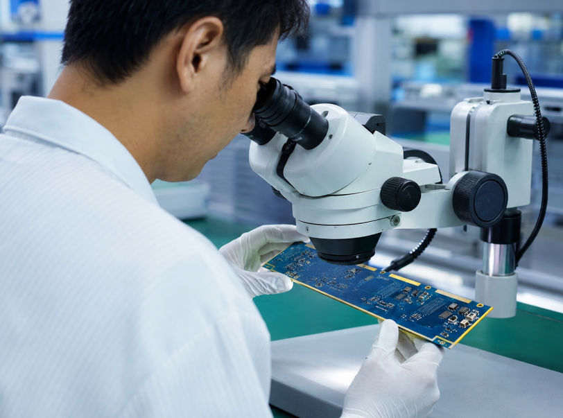
How Should PCB Edge Plating Quality Be Inspected?
PCB edge plating quality should be inspected through a clear process, not only by checking the board appearance. The inspection should confirm plating coverage, edge adhesion, electrical continuity, finish thickness and assembly fit.
Step 1: Check the plated edge visually
Inspect the plated edge under proper lighting and magnification. The edge should have continuous metal coverage without exposed laminate, dark spots, scratches, dents, rough burrs or missing plated areas.
Step 2: Confirm the plated area matches the drawing
Compare the finished board with the mechanical layer and fabrication notes. Check whether the correct edge is plated, whether plating starts and stops at the marked position, and whether non-plated tab areas are acceptable.
Step 3: Test electrical continuity
Use an electrical test to confirm that the plated edge connects to the intended net, usually GND. Also check that it does not short to signal traces, power planes or unrelated internal copper layers.
Step 4: Measure surface finish thickness
For ENIG, hard gold or other finishes, use XRF testing when thickness control is required. This helps confirm whether nickel, gold or other finish layers meet the project specification.
Step 5: Check copper thickness and side-wall coverage
For high-reliability projects, cross-section inspection can be used to verify copper build-up on the side wall. This is useful when the edge is used for shielding contact, soldering or repeated mechanical contact.
Step 6: Inspect adhesion and peeling risk
Check whether the plated layer bonds firmly to the routed edge. Tape testing, cross-section review or controlled mechanical checks may be used when the product has vibration, friction or housing contact requirements.
Step 7: Check burrs and edge smoothness
Inspect the routed edge after final separation. Burrs, rough fibers or sharp metal edges may affect assembly, soldering, connector fit or metal housing contact. Severe burrs should be rejected or reviewed before assembly.
Step 8: Confirm dimensions and assembly clearance
Measure the board outline, plated edge thickness and critical contact area. This is important when the plated edge contacts a metal enclosure, spring clip, connector, shielding frame or module carrier board.
Step 9: Review solderability when needed
If the plated edge will be soldered, check wetting behavior and finish condition. Oxidation, contamination or uneven finish may cause poor solder flow on the side wall.
Step 10: Record inspection results before shipment
For production batches, inspection records should include visual findings, electrical test results, finish thickness data, cross-section results if required, and any approved tab marks or cosmetic limits.
A reliable inspection process should confirm that PCB edge plating is continuous, correctly connected, mechanically stable, dimensionally accurate and suitable for final assembly. Acceptance should follow the customer drawing, IPC-A-600 appearance criteria, IPC-6012 performance requirements and RoHS compliance when applicable.
FAQs About PCB Edge Plating
Q1: Can PCB edge plating be used on thin boards?
A1: Yes, but very thin boards need careful review because the side wall has less area for stable copper coverage. For thin PCB designs, the manufacturer should check board thickness, edge length, routing quality and copper support. If the edge is used for contact or shielding, enough mechanical strength is important to prevent edge damage during handling or assembly.
Q2: Will plated edges affect board outline tolerance?
A2: Yes, plated edges may slightly affect the final outline size because copper and finish are added to the routed side wall. This matters when the PCB fits into a metal housing, slot, spring clip or connector. For tight mechanical assemblies, the drawing should define both board outline tolerance and plated edge requirements before production.
Q3: Are small unplated marks acceptable on plated edges?
A3: Small unplated marks may appear where panel support tabs are removed. Whether they are acceptable depends on the contact function. If the plated edge only supports general grounding, small tab marks may be acceptable. If the area contacts a housing, clip or solder joint, tab positions should be moved away from functional zones.
Q4: Can PCB edge plating be used with rigid-flex PCB?
A4: It can be possible on the rigid section, but it is not suitable for flexible bend areas. The plated edge should stay on the rigid part where routing, copper plating and mechanical support are stable. For rigid-flex projects, the factory should review the stackup, transition area and bend zone before confirming edge plating feasibility.
Q5: Does PCB edge plating need special packaging?
A5: Yes, plated edges should be protected from scratches, oxidation and impact during shipment. Boards with ENIG or hard gold edges should be packed with separators, vacuum packaging or anti-static protection when required. If the plated edge is a contact surface, avoid board-to-board rubbing because it can damage the finish before assembly.
Q6: Can a plated edge be soldered directly to another metal part?
A6: Yes, if the finish is solderable and the contact area is designed for soldering. ENIG is commonly used for solderable edge applications. However, soldering to a side wall is less forgiving than soldering to a flat pad, so the design should provide enough exposed copper, proper solder access and stable mechanical support.
Q7: How should plated edges be handled during PCBA assembly?
A7: Operators should avoid scratching or clamping directly on functional plated edges. If the edge contacts a shield, frame or connector, damage can reduce conductivity or contact stability. During assembly, tooling, trays and fixtures should avoid plated contact areas. Visual inspection after assembly is useful for products with strict grounding or shielding requirements.
Q8: Is PCB edge plating suitable for high-volume production?
A8: Yes, but the design should be stable before mass production. High-volume orders need fixed panelization, approved tab locations, confirmed inspection criteria and consistent surface finish control. A prototype may pass electrically, but batch production still requires process control to avoid variation in plated coverage, burrs and contact areas.
Q9: What should be confirmed before using edge plating for a metal housing?
A9: Confirm the contact location, housing pressure, surface finish, board tolerance and grounding net. The plated edge should line up with the housing contact area, and tab marks should not fall on the contact point. If the housing applies pressure, the finish and copper adhesion should be strong enough for repeated assembly.
Q10: Can PCB edge plating improve ESD protection?
A10: It may help when connected to chassis ground or system ground, but it should not be treated as a complete ESD solution alone. ESD protection still depends on grounding path, protection components, enclosure design and discharge route. Edge plating can support a better grounding structure when it is correctly connected and positioned.
Q11: Does PCB edge plating require a special surface cleaning process?
A11: Yes, the routed side wall must be clean before copper deposition. Resin dust, glass fiber debris, oxidation or burrs can weaken copper adhesion. Poor cleaning may lead to peeling, exposed laminate or uneven plating. This is why edge preparation before electroless copper is one of the key process controls.
Q12: Can edge plating be added after the PCB is already finished?
A12: In most cases, no. Reliable edge plating must be planned before plating and routing are completed. After the PCB is finished, the side wall usually lacks the required conductive seed layer and controlled copper build-up. Manual repair or post-treatment cannot provide the same adhesion, thickness and reliability as factory edge plating.
Conclusion
PCB edge plating works best when the design is clear before production: marked plated areas, correct net connection, enough copper overlap, safe pullback, proper solder mask opening, suitable finish and strict inspection. ENIG is a practical choice for most grounding and shielding edges, while hard gold is better for repeated contact or wear areas.
Need custom PCB edge plating for your next project? EBest Circuit is a China source factory supporting PCB fabrication, PCBA assembly, DFM review and global delivery. Send your Gerber files, drawings and quantity requirements to sales@bestpcbs.com for a fast quotation.
You may also like


Tags: edge plating in pcb, PCB Edge Plating Guidelines, pcb edge plating process, pcb edge plating thickness