

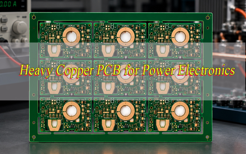
Heavy copper PCB for power electronics is used in circuits that carry high current, generate heat, or operate under repeated load changes. It is common in power supplies, motor drives, inverters, battery systems, EV chargers, converters and industrial control modules.
This guide explains copper thickness, current capacity, thermal control, trace width, via design, stackup, fabrication risks, reliability testing, cost factors and supplier selection for heavy copper PCB projects.
What Is Heavy Copper PCB for Power Electronics?
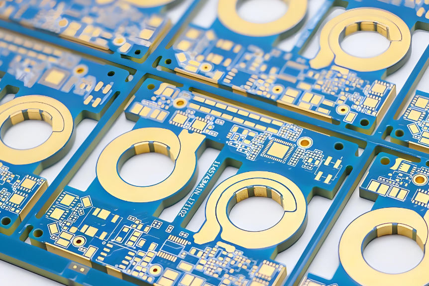
Heavy copper PCB for power electronics uses thicker copper than standard PCB to carry higher current and control heat. Standard PCB often uses 1 oz copper, while heavy copper PCB usually starts from 2 oz and can reach 3 oz, 4 oz, 6 oz or higher.
Thicker copper increases the conductor cross-section, which lowers resistance and reduces voltage drop. It also helps spread heat from MOSFETs, IGBTs, rectifiers, connectors and other power components.
Heavy copper PCB is commonly used in power supplies, motor drives, battery systems, converters and industrial control equipment. It is selected when standard copper cannot meet current load, thermal rise or mechanical reliability requirements.
Why Do Power Electronics Use Heavy Copper PCB?
Power electronics use heavy copper PCB because power circuits must carry current safely without excessive heat, voltage drop or conductor stress. Thin copper may work for control signals, but it is often not enough for high-current power paths.
Heavy copper improves three key areas: current carrying capacity, thermal spreading and mechanical strength. These points directly affect efficiency, reliability and service life in power conversion products.
Key functions include:
- Carrying continuous and peak current with lower resistance
- Reducing conductor temperature rise in compact layouts
- Improving heat spreading near power semiconductors
- Strengthening solder joints around connectors and terminals
- Supporting long-duty operation in industrial environments
- Reducing failure risk during thermal cycling and vibration
For power electronics, copper thickness should be selected from real current, temperature rise and layout space, not from a fixed default value.
What Problems Does Heavy Copper PCB Solve in High-Current Circuits?
Heavy copper PCB solves failures caused by undersized conductors, weak heat spreading and poor power-path design. These problems often appear after prototype testing, thermal testing or early field operation.
The most common issue is localized overheating. It can occur near MOSFETs, rectifiers, terminals, narrow copper necks, via transitions or high-current connectors. Once heat concentrates in one area, solder joints, laminate and plated holes may degrade faster.
Heavy copper helps control:
- Voltage drop across long or narrow power traces
- Copper heating caused by high current density
- Hot spots around switching and rectifier sections
- Barrel cracking in stressed plated through holes
- Pad lifting near high-current connectors
- Solder joint fatigue under repeated load cycles
Heavy copper cannot correct poor circuit topology, weak airflow or unsuitable components. It must be used with correct layout, stackup, material and thermal design.
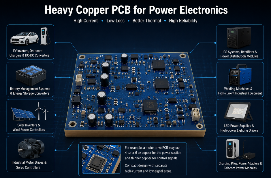
Where Is Heavy Copper PCB Used in Power Electronics Applications?
Heavy copper PCB for power electronics is used where current flow, switching loss and heat density are higher than standard PCB can handle. These applications often combine power devices, magnetic components, terminals and control circuits on one board.
Common applications include:
- EV inverters, on-board chargers and DC-DC converters
- Battery management systems and energy storage converters
- Solar inverters and wind power controllers
- Industrial motor drives and servo controllers
- UPS systems, rectifiers and power distribution modules
- Welding machines and high-current industrial equipment
- LED power supplies and high-power lighting drivers
- Charging piles, power adapters and telecom power modules
For example, a motor drive PCB may use 4 oz or 6 oz copper for the power section and thinner copper for control signals. This keeps the board compact while separating high-current and low-signal areas.
What Copper Thickness Is Suitable for Power Electronics PCB?
Copper thickness depends on current, temperature rise, trace width, layer position, cooling method and board size. A higher copper weight does not automatically mean a better design. Oversized copper can increase cost, reduce spacing capability and make fabrication harder.
As a practical range, 2 oz copper is used for moderate power circuits, 3 oz–4 oz copper is common for high-current power boards, and 6 oz or above is used when current density is high or board space is limited.
| Copper | Thickness | Common Use |
|---|---|---|
| 2 oz | 70 µm | Moderate current power PCB |
| 3 oz | 105 µm | LED drivers, converters, chargers |
| 4 oz | 140 µm | Motor drives, battery modules |
| 6 oz | 210 µm | High-current industrial power |
| 10 oz+ | 350 µm+ | Busbar-level power paths |
Copper selection should be verified by trace width calculation, thermal simulation and prototype testing. For safety, check both continuous current and peak current, because many power products experience surge load during startup, switching or overload conditions.
How Does Heavy Copper PCB Improve Current Carrying Capacity?
Heavy copper PCB improves current carrying capacity by increasing the copper cross-section. A thicker copper path has lower resistance, which reduces heat generation and voltage drop under the same current load.
Key design points include:
- Copper thickness affects current capacity directly. Common heavy copper options include 2 oz, 3 oz, 4 oz and 6 oz. Higher copper weight allows more current, but it also increases cost and fabrication difficulty.
- Trace width must match real current load. A thick copper trace can still overheat if the width is too narrow. Designers should calculate continuous current, peak current and acceptable temperature rise before finalizing layout.
- External layers usually dissipate heat better. Outer copper layers are closer to airflow, solder mask openings and heatsink contact areas, so they often carry heat away faster than internal layers.
- Current bottlenecks must be avoided. Narrow copper necks near terminals, MOSFETs, fuses, connectors or shunt resistors can become hot spots even when the rest of the copper area is large.
- Via transitions need enough current capacity. When current moves between layers, one or two small vias are usually not enough. Via arrays, larger hole sizes or plated slots may be required.
- Connector ratings must match PCB current paths. The PCB copper may carry high current, but weak terminals, solder joints or connector pins can still limit the final design.
How Does Heavy Copper PCB Help Thermal Management?
Heavy copper PCB helps thermal management by reducing conductor loss and spreading heat across larger copper areas. It is especially useful in power electronics where MOSFETs, IGBTs, rectifiers, inductors and connectors generate concentrated heat.
Key thermal design points include:
- Lower resistance reduces heat generation. Thicker copper creates a lower-resistance path, so less heat is produced when current flows through the PCB.
- Large copper areas spread heat faster. Wide copper pours around power components help move heat away from local hot spots and reduce temperature concentration.
- Thermal vias improve vertical heat transfer. Vias placed under or near hot pads can move heat to inner layers, bottom copper areas, heatsinks or metal base structures.
- Hot components need direct heat paths. MOSFET drain pads, rectifier pads, power resistors and terminals should connect to copper areas that can transfer heat efficiently.
- Copper balance helps temperature stability. Balanced copper distribution reduces warpage and supports more even heat spreading during operation.
- Material selection still matters. High-Tg FR-4, CTI-rated laminate, IMS or other thermal materials may be required when working temperature or voltage stress is high.
- Real load testing is necessary. Thermal simulation is useful, but final temperature rise should be checked under real current, enclosure and cooling conditions.
Heavy copper improves heat spreading, but it does not replace heatsinks, airflow, thermal pads or proper enclosure design in high-power systems.
What Materials Are Used for Heavy Copper PCB in Power Electronics?
Materials must support heat, insulation, copper adhesion and mechanical stress. Copper thickness is only one part of the design. If the laminate cannot handle temperature or voltage stress, the board may still fail.
FR-4 is suitable for many industrial power boards. For higher temperature, higher voltage or stricter reliability requirements, designers may use High-Tg FR-4, CTI-rated laminate, IMS substrate or ceramic-filled material.
| Material | Feature | Suitable Project |
|---|---|---|
| High-Tg FR-4 | Better heat resistance | Industrial power supplies |
| CTI-rated laminate | Improved insulation safety | High-voltage power PCB |
| IMS substrate | Metal-backed heat path | LED and power modules |
| Ceramic-filled laminate | Thermal and dimensional stability | High-reliability power boards |
| Heavy copper foil | High current path | Motor drives, converters |
| RoHS finish | Lead-free compliance | EU and global projects |
Material selection should match operating temperature, working voltage, insulation requirement, flame rating, assembly process and export compliance. For Europe and North America, RoHS, UL and customer-specific reliability requirements are often part of the procurement review.
How Should Trace Width and Spacing Be Designed for Heavy Copper PCB?
Trace width and spacing should be designed from current, voltage, copper thickness, temperature rise and fabrication capability. Heavy copper cannot follow the same spacing rules as standard 1 oz PCB because thick copper is harder to etch and control.
Key layout rules include:
- Trace width should be based on current and temperature rise. Wider traces reduce resistance and help control heat. The design should consider continuous current, peak current and maximum allowed PCB temperature.
- Spacing should be based on voltage and safety requirements. High-voltage circuits need enough clearance and creepage distance to prevent arcing, leakage current and insulation failure.
- Copper thickness affects minimum spacing. As copper becomes thicker, etching becomes more difficult. Tight spacing between thick copper traces may increase undercut, short circuit or solder mask coverage risk.
- Use copper pours for main power paths. Large copper pours are better than long narrow traces for high-current circuits because they reduce resistance and spread heat more evenly.
- Avoid sharp corners and narrow necks. Sharp angles and sudden width changes can concentrate current and heat. Smooth transitions are better for power paths.
- Separate power and signal areas. High-current switching paths can create noise. Sensitive signal traces should be kept away from MOSFET switching nodes, inductors and high-current loops.
- Confirm limits before final layout. Minimum trace width, spacing, copper thickness and solder mask capability should be checked with the PCB manufacturer before Gerber release.
What Via Design Rules Apply to High-Current PCB?
Via design is critical in high-current PCB because vias must carry current, transfer heat and withstand thermal stress. Poor via design can cause overheating, barrel cracking, uneven current sharing or failure during thermal cycling.
Key via design rules include:
- Use via arrays for high-current transfer. One small via is rarely enough for a power path. Multiple vias should be used when current moves between copper layers.
- Increase finished hole size when possible. Larger vias provide more plating area and better current capacity. They also improve mechanical strength compared with very small vias.
- Check finished copper plating thickness. Via reliability depends on actual plated hole wall thickness, not only drill size. Cross-section inspection is useful for heavy copper PCB.
- Place vias close to the current path. Power vias should be located near terminals, MOSFETs, rectifiers and other high-current areas to reduce path length and resistance.
- Use thermal vias under hot components. Thermal vias can move heat from top copper to bottom copper, internal copper planes or heatsink contact areas.
- Avoid using signal vias as power vias. Small signal vias are not designed for high current and may create localized heating or early failure.
- Consider plated slots for terminals. For very high-current connectors or press-fit terminals, plated slots may provide stronger current transfer and mechanical support than small round vias.
- Keep via arrays balanced. Uneven via placement can cause unequal current sharing and local overheating. Symmetrical via groups usually perform better.
How Should Stackup and Copper Balance Be Planned?
Stackup and copper balance should be planned before layout is finalized. In heavy copper PCB fabrication, poor copper balance can cause warpage, uneven lamination pressure, soldering defects and unstable assembly yield.
Key planning rules include:
- Keep copper distribution balanced. Avoid placing a large heavy copper area on one layer while the opposite layer has very little copper. Uneven copper can pull the board during lamination and reflow.
- Separate power and signal functions. High-current layers should be kept away from sensitive analog, communication or control signals when possible. This reduces noise coupling and improves layout stability.
- Use proper dielectric thickness for voltage insulation. High-voltage power electronics may require larger spacing between copper layers to prevent breakdown and leakage risk.
- Place return paths close to switching current paths. Short return paths help reduce loop area, switching noise and electromagnetic interference in converters, motor drives and inverters.
- Confirm finished copper thickness. Base copper and plated copper are not the same. Buyers should confirm the final copper thickness after plating, especially for 3 oz, 4 oz and 6 oz boards.
- Review stackup before Gerber release. Stackup changes after layout may affect trace width, impedance, spacing, via structure and production cost.
Case example:
A motor drive PCB used 4 oz copper on outer power layers and thinner copper for control routing. The first layout had large copper pours only on the top layer, which caused warpage risk during assembly. After DFM review, copper was redistributed across opposite layers, return paths were adjusted, and thermal vias were added near MOSFET areas. The revised stackup improved flatness, heat distribution and batch production stability.
What Manufacturing Challenges Affect Heavy Copper PCB Fabrication?
Heavy copper PCB fabrication is more difficult than standard PCB production because thick copper affects etching, plating, lamination, drilling and solder mask application. These process risks should be reviewed during DFM before tooling.
Common manufacturing challenges include copper undercut, uneven plating, resin voids, poor solder mask coverage, warpage, hole wall defects and dimensional drift. The risk becomes higher when copper thickness increases or when trace spacing is too tight.
Main control points include:
- Adjust trace spacing for thick copper etching
- Balance copper distribution across the panel
- Control resin flow during lamination
- Improve plating uniformity in vias and through holes
- Apply suitable solder mask thickness around copper steps
- Inspect cross-sections for plating and lamination quality
- Run thermal stress tests for high-reliability projects
A practical process flow starts with DFM review, then material preparation, inner layer imaging, etching, lamination, drilling, copper plating, outer layer imaging, final etching, solder mask, surface finish, routing, electrical testing and final inspection.
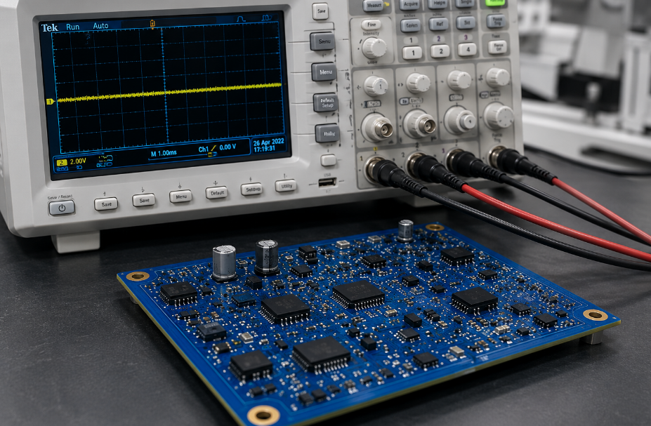
What Quality Tests Are Needed for Heavy Copper PCB Reliability?
Heavy copper PCB should be tested for copper thickness, plated hole quality, electrical continuity, solderability, thermal resistance and final dimensions. Thick copper boards carry higher current, so hidden defects can become serious reliability risks during operation.
Important quality tests include:
- AOI inspection. Checks open circuits, shorts, conductor shape, over-etching, under-etching and pattern defects before shipment.
- 100% electrical testing. Confirms circuit continuity and insulation performance. This is required for high-current PCB because open or short defects can damage power modules.
- Copper thickness measurement. Verifies whether finished copper meets the required specification, such as 2 oz, 3 oz, 4 oz or 6 oz.
- Cross-section inspection. Checks hole wall plating thickness, copper bonding, resin filling, lamination quality and possible barrel defects.
- Thermal stress testing. Exposes the PCB to heat stress to check delamination, blistering, hole wall cracking and laminate stability.
- Solderability testing. Confirms whether pads and terminals can be soldered properly during assembly, especially after storage or surface finish processing.
- Ionic contamination testing. Checks whether chemical residues remain on the board. Excessive residue may cause leakage, corrosion or reliability problems.
- Dimensional inspection. Verifies board outline, slot size, hole position, thickness and tolerance before assembly.
- Visual inspection. Reviews solder mask coverage, copper exposure, surface finish quality, scratches, dents and edge defects.
- Final quality report. For power electronics projects, buyers can request inspection data for copper thickness, cross-section, electrical testing and thermal stress results.
What Factors Affect Heavy Copper PCB Cost?
Heavy copper PCB cost is affected by copper weight, layer count, board size, material grade, hole density, copper balance, surface finish, tolerance, testing and order quantity. The thicker the copper, the higher the material cost and process difficulty.
Cost also increases when the design has tight spacing, dense vias, specialty laminate, ENIG finish, strict cross-section requirements or low-volume production. For very thick copper, fabrication time and yield risk become important pricing factors.
Main cost factors include:
- Copper thickness and finished copper requirement
- Board layer count and stackup complexity
- High-Tg, CTI-rated or specialty laminate
- Minimum trace width and spacing
- Hole density, slot design and plating demand
- Solder mask difficulty around thick copper
- ENIG, HASL lead-free or other surface finish
- Cross-section, thermal stress and reliability tests
- Prototype, small batch or volume production quantity
The lowest unit price is not always the lowest project cost. A poor design may cause overheating, failed samples, delayed approval or batch rejection. Heavy copper PCB cost should be reviewed with performance, yield and reliability risk together.
How to Choose a Heavy Copper PCB Manufacturer for Power Electronics?
Choose a heavy copper PCB manufacturer that can review current load, copper thickness, trace spacing, via capacity, stackup balance and testing requirements before production. Heavy copper projects require process control, DFM support and reliability testing, not only basic PCB fabrication.
Selection points include:
- Check real heavy copper experience. The manufacturer should have experience with 2 oz, 3 oz, 4 oz, 6 oz or thicker copper for power electronics, motor drives, converters and industrial power modules.
- Ask for DFM review before production. A qualified factory should check copper spacing, solder mask coverage, via structure, plating risk, stackup balance and possible warpage issues.
- Confirm finished copper capability. The supplier should explain base copper, plated copper and final copper thickness clearly, not only quote a general copper weight.
- Review testing capability. Cross-section inspection, electrical testing, copper measurement and thermal stress testing are important for heavy copper PCB reliability.
- Check material and compliance support. For export projects, the manufacturer should support RoHS, UL-related material requirements, High-Tg laminate and IPC acceptance criteria when required.
- Evaluate prototype-to-batch consistency. A good supplier should keep the same engineering data, material selection and process controls from sample approval to mass production.
- Confirm communication speed. Heavy copper PCB often needs engineering clarification before production. Slow feedback can delay prototypes, testing and batch delivery.
- Choose a real China source factory. EBest supports custom heavy copper PCB prototypes, small batches and volume production with global delivery, without claiming overseas factories, warehouses or local branches.
FAQs About Heavy Copper PCB for Power Electronics
Q1: What is the minimum copper thickness for heavy copper PCB?
A1: Heavy copper PCB usually starts from 2 oz copper, which equals about 70 µm copper thickness. Many power electronics projects use 3 oz, 4 oz or 6 oz depending on current load, trace width, temperature rise and board size. The correct copper thickness should be calculated from actual electrical and thermal conditions.
Q2: Is thicker copper always better for power electronics PCB?
A2: No. Thicker copper can improve current capacity and heat spreading, but it also increases cost, etching difficulty and spacing limitations. A 6 oz board may not be necessary if 3 oz or 4 oz copper already meets the current and temperature targets. The best choice balances performance, manufacturability and cost.
Q3: Can heavy copper PCB be used with SMT assembly?
A3: Yes. Heavy copper PCB can support SMT assembly, but pad design, solder mask thickness and thermal balance must be checked carefully. Thick copper absorbs more heat during soldering, so reflow profile, solder paste volume and component thermal sensitivity should be reviewed before assembly.
Q4: What information should buyers provide before quoting?
A4: Buyers should provide Gerber files, drill files, stackup, copper thickness, board thickness, material, surface finish, quantity and testing requirements. For power electronics PCB, it is better to also provide working current, peak current, voltage, temperature rise target and operating environment.
Q5: Why does heavy copper PCB need DFM review?
A5: Heavy copper PCB needs DFM review because thick copper affects etching, plating, solder mask coverage, lamination and warpage control. DFM review can identify spacing risks, narrow copper necks, weak vias, poor copper balance and difficult solder mask areas before production starts.
Q6: What surface finish is commonly used for heavy copper PCB?
A6: ENIG, HASL lead-free, immersion tin and OSP can be used. ENIG is often selected for stable solderability and fine-pitch components, while HASL lead-free may be suitable for simpler power boards. The final choice depends on component type, storage time, soldering process, RoHS requirement and cost.
Q7: Can heavy copper PCB handle high voltage?
A7: Heavy copper PCB can be used in high-voltage power electronics, but voltage safety depends on clearance, creepage, dielectric thickness, material CTI and coating, not copper thickness alone. Designers should define working voltage, peak voltage and insulation requirement before layout.
Q8: Why do heavy copper PCB vias fail?
A8: Via failure is often caused by insufficient plating thickness, small via size, poor drilling quality, thermal cycling or excessive current concentration. High-current PCB should use suitable via diameter, via arrays, proper plating control and cross-section inspection to reduce barrel cracking and overheating risk.
Q9: Can heavy copper PCB reduce PCB temperature?
A9: Heavy copper can reduce conductor loss and heat concentration, but it cannot replace the full thermal system. High-power designs may still require heatsinks, airflow, thermal pads, metal baseplates or enclosure cooling. Final temperature should be tested under real current and working conditions.
Q10: What causes warpage in heavy copper PCB?
A10: Warpage is often caused by unbalanced copper distribution, uneven layer structure, high copper weight on one side, poor lamination control or unsuitable panel design. Balanced stackup and copper distribution are important for 4 oz, 6 oz and thicker copper boards.
Q11: Is heavy copper PCB suitable for prototypes?
A11: Yes. Heavy copper PCB prototypes are useful for checking current capacity, temperature rise, solderability, mechanical fit and assembly performance before batch production. Prototype testing can prevent redesign and reduce risk before larger power electronics orders.
Q12: What industries commonly use heavy copper PCB?
A12: Heavy copper PCB is widely used in EV chargers, battery systems, solar inverters, UPS systems, motor drives, welding machines, industrial power supplies, LED drivers and telecom power modules. These products usually require high current paths, stable heat spreading and stronger long-term reliability.
Q13: Can EBest manufacture custom heavy copper PCB?
A13: Yes. EBest supports custom heavy copper PCB manufacturing for prototypes, small batches and volume production. We can review copper thickness, stackup, trace width, spacing, via structure, solder mask coverage and testing requirements before production to help reduce project risk.
Heavy copper PCB for power electronics should be selected from real current load, voltage level, temperature rise, copper thickness, stackup and reliability requirements. A stable design depends on more than thick copper; trace width, spacing, via structure, material, solder mask and testing must work together.
If you need thick copper boards for power supplies, motor drives, inverters, battery systems, EV chargers or industrial power modules, EBest Circuit can support custom heavy copper PCB prototypes and batch production from China with global delivery. Send your Gerber files, stackup and technical requirements to sales@bestpcbs.com for a quotation.
You may also like


Tags: heavy copper pcb, heavy copper pcb design, Heavy Copper PCB for Power Electronics