

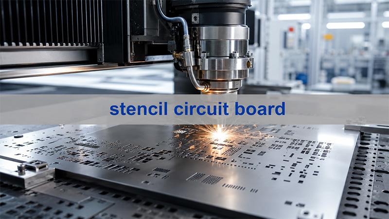
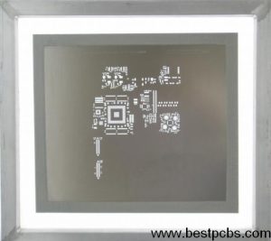
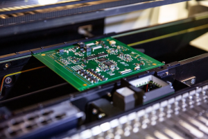
A stencil circuit board usually refers to a PCB solder paste stencil used to print solder paste onto a circuit board before SMT assembly. In this process, a thin stainless steel stencil is aligned over the PCB, and solder paste is pushed through small laser-cut openings onto the surface-mount pads. This step matters because solder paste volume and position directly affect solder joint quality, fine-pitch component reliability, and overall PCBA yield.
This guide covers PCB stencil basics, solder paste printing, stencil types, thickness selection, laser stencil benefits, common SMT defects, and practical design rules for better assembly quality.
At EBest Circuit, we treat stencil design as part of the complete SMT PCBA process, not as a separate accessory. Our team reviews Gerber files, BOM data, component packages, PCB surface finish, and assembly requirements to help customers reduce solder defects and improve production consistency from prototype to batch assembly. For stencil-related PCB assembly support, you can send your files or questions to sales@bestpcbs.comfor a practical engineering review.
What Is a Stencil Circuit Board and How Is It Used in SMT Assembly?
A stencil circuit board usually refers to the solder paste printing process used before SMT assembly. In professional PCB manufacturing, the stencil is not the circuit board itself. It is a precision tool placed over the PCB to print solder paste onto the surface-mount pads.
In the PCB industry, this tool may also be called a PCB stencil, solder stencil, solder paste stencil, circuit board stencil, or printed circuit board stencil. These terms usually describe the same item when people are talking about SMT assembly.
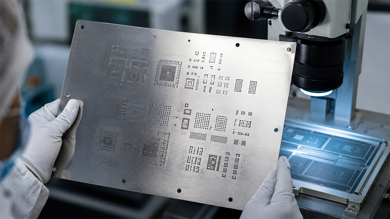
The stencil has small laser-cut openings called apertures. These apertures match the SMT pads on the printed circuit board. During printing, solder paste is pushed across the stencil with a squeegee. The paste passes through the apertures and forms controlled deposits on the PCB pads. After that, SMT components are placed onto the paste and soldered during the reflow process.
This step may look simple, but it directly affects solder joint quality. A good PCB stencil controls where the paste goes, how much paste is deposited, and how consistent the paste volume remains across the board. If the stencil design or printing process is not well controlled, defects such as solder bridging, insufficient solder, tombstoning, solder balls, open joints, or unstable fine-pitch assembly may appear.
A well-designed solder paste stencil helps improve:
- Solder paste position accuracy
- Solder paste volume consistency
- Fine-pitch component assembly
- Reflow solder joint reliability
- First-pass yield
- SMT production repeatability
- Rework reduction
For prototype boards, engineers may use a frameless solder stencil and apply paste manually. For medium and high-volume production, a framed laser stencil and a printed circuit board stencil printer are more suitable because they provide better tension, alignment, and repeatability.
In commercial PCB assembly, the stencil should be reviewed together with the PCB layout, BOM, component package types, board finish, and assembly process. A PCB stencil is not only a paste application tool. It is part of the SMT process control system. A well-designed stencil gives the assembly line a cleaner starting point and helps the whole production flow run more smoothly.
What Are the Main Types of PCB Stencils?
Different PCB projects need different stencil types. The right choice depends on production volume, component density, pad geometry, board size, and printing method.
| PCB Stencil Type | Best For | Main Advantage | Typical Application |
|---|---|---|---|
| Framed PCB stencil | Medium to high-volume production | Stable tension and repeatable printing | Automatic SMT stencil printer |
| Frameless PCB stencil | Prototype and small batch assembly | Lower cost and easy storage | Manual printing or reusable frame |
| Laser stencil | Most professional SMT projects | Accurate apertures and clean paste release | Fine-pitch SMT assembly |
| Step stencil | Mixed component paste volume needs | Different thickness in selected areas | Boards with small ICs and large connectors |
| Nano-coated stencil | Dense or high-reliability boards | Better paste release and easier cleaning | 0201, QFN, BGA, fine-pitch ICs |
| Rework stencil | Local component repair | Applies paste to one selected area | BGA, QFN, connector repair |
For most modern SMT projects, a stainless steel laser stencil is the preferred option. It offers better aperture accuracy than low-cost plastic or manually cut stencils. This matters when the board includes fine-pitch ICs, small passives, QFNs, BGAs, or compact modules.
For early prototypes, a simple solder stencil may be enough. For repeat production, a more controlled stencil design is usually worth the investment.
Framed vs. Frameless PCB Stencil: Which One Should You Choose?
One of the most common decisions is whether to choose a framed or frameless PCB stencil.
A framed PCB stencil is mounted permanently inside an aluminum frame. The frame keeps the stencil under tension, which helps maintain flatness during printing. This type is widely used with automatic or semi-automatic stencil printers.
A frameless PCB stencil is a stainless steel sheet without a permanent frame. It is lighter, easier to ship, and usually more affordable. It can be used manually or placed into a reusable tensioning frame.
| Item | Framed PCB Stencil | Frameless PCB Stencil |
|---|---|---|
| Cost | Higher | Lower |
| Printing stability | Excellent | Good with proper fixture |
| Storage space | Larger | Compact |
| Best volume | Medium to high volume | Prototype to small batch |
| Typical method | Automatic stencil printer | Manual or semi-automatic printing |
| Repeatability | Strong | Depends on fixture and operator |
| Shipping | Heavier | Easier and cheaper |
Choose a framed stencil if your project needs repeat production, stable paste printing, and automated SMT assembly.
Choose a frameless stencil if your project is still in prototype validation, small batch testing, or engineering verification.
For companies moving from prototype to volume production, it is common to start with a frameless stencil and later switch to a framed laser stencil once the PCB design is stable.
Why Are Laser-Cut Stencils Preferred for Fine-Pitch SMT Components?
A laser-cut stencil is made by cutting apertures into stainless steel according to the PCB paste layer. Compared with simple plastic stencils or low-precision cutting methods, laser cutting provides much cleaner aperture geometry.
Fine-pitch SMT components need very controlled solder paste deposits. If the aperture is rough, too large, or poorly shaped, paste release becomes unstable. This can affect IC pins, small passive components, QFN pads, BGA pads, and high-density layouts.
Laser-cut PCB stencils are preferred because they offer:
- More accurate aperture size
- Cleaner aperture walls
- Better solder paste release
- Improved fine-pitch printing
- Stronger repeatability
- Better support for small SMT packages
- Less risk of paste smearing
For 0201 components, 01005 components, QFNs, BGAs, and fine-pitch connectors, aperture wall quality matters. Smooth aperture walls help solder paste release cleanly from the stencil instead of sticking inside the openings.
For advanced assemblies, nano-coating can also be added to the stencil surface. This improves paste release and reduces cleaning frequency, especially when the stencil has many small apertures.
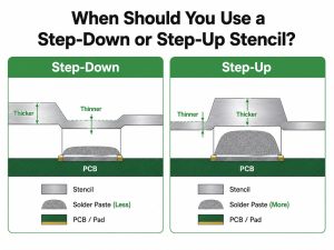
What Stencil Thickness Should You Use for a Circuit Board?
Stencil thickness controls solder paste volume. A thicker stencil deposits more paste. A thinner stencil deposits less paste and is often better for fine-pitch components.
There is no single stencil thickness that fits every PCB. The right thickness depends on component package types, pad size, board design, and assembly requirements.
| Stencil Thickness | Common Use |
|---|---|
| 0.08 mm / 3 mil | Ultra-fine pitch, 01005, very small pads |
| 0.10 mm / 4 mil | Fine-pitch ICs, 0201 components |
| 0.12 mm / 5 mil | General SMT assembly with moderate density |
| 0.15 mm / 6 mil | Standard SMT boards with larger components |
| 0.18 mm / 7 mil or above | High paste volume pads, larger terminals, special applications |
For many standard SMT boards, 0.12 mm or 0.15 mm is common. However, boards with very small components may need thinner stencils to avoid excess paste. Boards with large connectors, power components, or shield pads may need more paste.
This creates a challenge when one PCB has both tiny fine-pitch components and large pads. In that case, a step stencil may be a better choice. A step stencil allows selected areas to be thinner or thicker, so each component receives the right paste volume.
Stencil thickness should not be selected only by habit. It should be reviewed according to the actual PCB design.
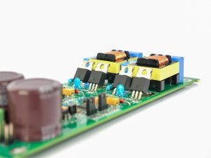
What Are Common SMT Printing Defects and How Can a Quality Stencil Fix Them?
Many SMT defects begin during solder paste printing. A quality stencil cannot replace good process control, but it gives the assembly process a much better starting point.
| SMT Printing Defect | Common Cause | How a Better Stencil Helps |
|---|---|---|
| Solder bridging | Too much paste or poor aperture design | Reduces excess paste and improves aperture control |
| Insufficient solder | Small aperture, poor paste transfer, clogged openings | Improves paste release and deposit consistency |
| Tombstoning | Uneven paste volume or thermal imbalance | Supports balanced paste deposits on both pads |
| Solder balls | Excess paste, smearing, poor cleaning | Improves edge definition and print cleanliness |
| Open joints | Low paste volume or poor contact | Helps maintain proper paste height |
| QFN voiding | Poor thermal pad paste design | Uses windowpane aperture design for better outgassing |
| Paste misalignment | Poor stencil positioning or unstable fixture | Framed stencil and printer alignment improve repeatability |
For example, QFN thermal pads should not always be printed as one large solder paste block. A segmented windowpane pattern can improve paste control and reduce voiding. Fine-pitch IC pads may need aperture reduction to prevent bridging. Large pads may need modified openings to avoid floating or excessive solder.
Good stencil design is practical engineering work. It is not only file processing.
Manual vs. Automatic PCB Stencil Printing: Which Method Fits Your Project?
PCB stencil printing can be done manually, semi-automatically, or with an automatic printed circuit board stencil printer. The best method depends on your project stage and production volume.
Manual printing is common for prototypes. The operator aligns the stencil with the PCB, applies solder paste, and uses a squeegee to spread the paste across the stencil. This method is flexible and affordable, but it depends heavily on operator skill.
Automatic stencil printing is used in professional SMT production. A printed circuit board stencil printer controls alignment, squeegee pressure, print speed, stencil separation, and cleaning cycles. For dense boards or repeated production, this method gives much better consistency.
| Printing Method | Best For | Advantage | Limitation |
|---|---|---|---|
| Manual stencil printing | Prototypes and simple boards | Low cost and quick setup | Operator-dependent |
| Semi-automatic printing | Small to medium batches | Better control than manual printing | Still needs setup skill |
| Automatic stencil printing | Volume SMT production | High repeatability and throughput | Higher equipment cost |
Some search terms describe this equipment as an SMT PCB solder paste stencil printing circuit board printing machine. In production language, it is usually called an SMT stencil printer or solder paste printer.
For commercial PCB assembly, automatic stencil printing is usually preferred because it reduces variation between boards. This is especially important for medical electronics, industrial control boards, communication modules, automotive electronics, and other reliability-focused applications.
How Should You Use a Solder Stencil Squeegee Correctly?
The solder stencil squeegee has a direct effect on paste filling and print quality. Even with a good stencil, poor squeegee technique can cause incomplete deposits, smearing, or inconsistent paste height.
Several factors should be controlled during the solder stencil squeegee circuit board process.
Squeegee angle
A typical angle is around 45° to 60°. This helps the solder paste roll smoothly across the stencil and fill the apertures properly.
Printing pressure
Pressure should be enough to wipe the stencil surface clean and fill the apertures. Too much pressure may scoop paste out of openings or damage the stencil over time.
Printing speed
A stable speed helps maintain a smooth paste roll. Very fast printing may leave incomplete deposits, while very slow printing may affect paste behavior.
Paste condition
Solder paste should be stored, warmed, and mixed according to supplier recommendations. Paste that is too dry or poorly handled can affect release quality.
PCB support
The board should be fully supported under the stencil. If the PCB flexes during printing, solder paste thickness may become uneven.
Stencil separation
After printing, the stencil should lift away cleanly. Good separation helps keep the paste deposit shape intact.
For manual prototype printing, it is helpful to use a flat fixture, proper board stops, and steady squeegee movement. For production, the printer should control pressure, speed, alignment, and cleaning cycle.
What PCB Stencil Design Rules Should Engineers Check Before Ordering?
Before ordering a circuit board stencil, engineers should review more than the paste layer. The stencil must match the actual assembly process.
Important checks include:
- Correct Gerber paste layer
- Accurate PCB outline
- Proper fiducials for alignment
- Suitable stencil thickness
- Aperture reduction for fine-pitch ICs
- Rounded aperture corners for better paste release
- Windowpane design for QFN thermal pads
- Paste opening adjustment for large pads
- Step stencil requirement for mixed components
- Panelized PCB compatibility
- Tooling holes and rail clearance
- Nano-coating requirement for dense apertures
- Component package review
- Special notes for selective assembly
A PCB stencil should not always copy the CAD paste layer exactly. Some apertures need adjustment to improve manufacturability. For example, large exposed pads may need segmented openings, while fine-pitch pads may need reduced aperture width.
Engineers should also check the aperture area ratio. If the aperture is too small relative to stencil thickness, solder paste may not release well. This is one reason thin stencils are often used for small components.
For complex PCB assemblies, stencil review should be included in DFM before production begins.
How Should PCB Stencils Be Cleaned and Maintained?
Stencil cleaning and storage affect long-term printing quality. Even a well-made stencil can create defects if solder paste dries inside the apertures or residue remains on the surface.
Good stencil maintenance includes:
- Clean the stencil after use
- Use compatible cleaning solvents
- Remove paste from aperture walls
- Avoid scratching the stencil surface
- Store the stencil flat or in a protected rack
- Keep framed stencils away from impact
- Inspect for damaged apertures
- Follow printer cleaning intervals
- Control paste drying during long print runs
Fine-pitch stencils need closer cleaning control because small apertures clog more easily. If paste does not release fully, the printed pads may receive less solder than expected.
For production lines, under-stencil cleaning is often scheduled after a certain number of prints. The interval depends on solder paste type, stencil design, aperture density, and process requirements.
A clean stencil supports more stable solder paste deposits and better SMT yield.
Why Choose EBest Circuit for PCB Stencil and SMT Assembly Support?
Choosing the right PCB stencil is important, but stencil quality works best when it is connected with the full SMT assembly process. The stencil, solder paste, PCB finish, component package, printer setup, placement accuracy, reflow profile, and inspection plan all need to work together.
EBest Circuit, also known as Best Technology, supports PCB fabrication, PCB assembly, component sourcing, DFM review, SMT assembly, testing, and box-build services. For stencil-related projects, the engineering team can review Gerber files, BOM, pick-and-place files, and assembly drawings before production.
EBest Circuit can support:
- Custom PCB fabrication
- Solder paste stencil preparation
- Laser stencil support
- SMT assembly
- Component sourcing
- BOM optimization
- DFM review
- AOI inspection
- X-ray inspection
- Functional testing
- Prototype and batch production
- Engineering support for fine-pitch assembly
For customers working on medical electronics, industrial control, communication devices, automotive electronics, battery charger PCBs, IoT products, and power electronics, stencil design is part of the broader manufacturing quality plan. If your PCB has fine-pitch components, QFNs, BGAs, 0201 parts, dense routing, or strict reliability requirements, it is better to review stencil requirements before production starts. For custom PCB stencil or SMT assembly support, please feel free to send your Gerber files, BOM, and assembly requirements to sales@bestpcbs.com. The EBest Circuit team will be glad to review your project and provide a practical quotation.
FAQs About Stencil Circuit Board
1. What is a stencil circuit board?
A stencil circuit board usually refers to the solder paste printing process used for SMT assembly. A PCB stencil is placed over the board, and solder paste is printed through the stencil openings onto the SMT pads.
2. Is a PCB stencil necessary for SMT assembly?
Yes, a PCB stencil is strongly recommended for SMT assembly. It helps apply solder paste accurately and consistently, especially when the board has fine-pitch ICs, small passive components, QFNs, or BGAs.
3. What is the difference between a solder stencil and a PCB stencil?
In most SMT assembly discussions, solder stencil and PCB stencil mean the same thing. Both refer to the stencil used to apply solder paste onto printed circuit board pads.
4. What is a laser stencil?
A laser stencil is a stainless steel PCB stencil with apertures cut by laser. It provides accurate openings, smooth aperture walls, and reliable solder paste release for SMT assembly.
5. What stencil thickness should I choose?
Common PCB stencil thickness ranges from 0.08 mm to 0.18 mm. Standard SMT boards often use 0.12 mm or 0.15 mm, while fine-pitch boards may need thinner stencils.
6. What is a framed PCB stencil?
A framed PCB stencil is mounted inside an aluminum frame. It provides stable tension and is commonly used with automatic stencil printers for repeat production.
7. What is a frameless PCB stencil?
A frameless PCB stencil is a stainless steel stencil sheet without a permanent frame. It is often used for prototypes, small batches, or reusable frame systems.
8. Can I use a DIY solder paste stencil?
A DIY stencil may work for simple hobby boards with large components. For professional PCB assembly, a stainless steel laser-cut stencil is usually better because it provides stronger accuracy and repeatability.
9. How do you cover unused openings in a PCB stencil?
Unused stencil openings can be temporarily covered with Kapton tape. For repeat production, it is better to revise the paste layer and make a corrected stencil.
10. What causes solder bridging during stencil printing?
Solder bridging may happen when too much paste is printed, stencil thickness is unsuitable, aperture design is not optimized, or the stencil is misaligned.
11. What files are needed to order a PCB stencil?
Most suppliers need the Gerber paste layer, PCB outline, fiducial information, and panel data. For full SMT assembly review, BOM and pick-and-place files are also useful.
12. Are circuit board paint stencils the same as PCB solder stencils?
No. A circuit board paint stencil or circuit board airbrush stencil is usually used for decoration or artwork. A PCB solder stencil is a manufacturing tool used to apply solder paste during SMT assembly.
You may also like

Tags: circuit board stencil, PCB stencil, stencil circuit board