

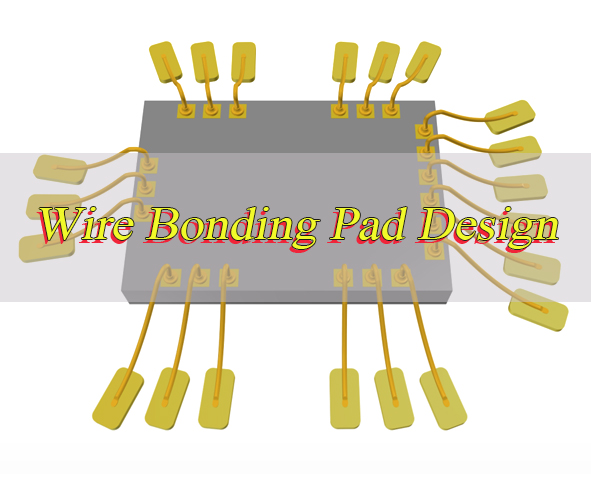
What critical factors determine the reliability and performance of wire bonding pad design, and how can designers avoid common pitfalls that lead to poor bonding quality and reduced yield? Wire bonding pad design is a foundational element of semiconductor and PCB manufacturing, directly impacting the mechanical strength, electrical conductivity, and long-term stability of interconnects.
This guideline breaks down the essential rules, materials, size specifications, and practical parameters needed to create robust, manufacturable wire bonding pad designs, addressing the most pressing questions and challenges faced during the design process.
What Are the Rules of Wire Bonding Pad Design in the Guideline?
Wire bonding pad design rules are non-negotiable standards that ensure compatibility with bonding processes, prevent structural failures, and maintain electrical performance. Key rules are as follows:
- Adhere to Manufacturer Design Rules: Strictly follow manufacturer-specific design rule documents, which outline minimum dimensions, spacing, and layout requirements tailored to their equipment and processes. This is the most critical rule to avoid compatibility issues.
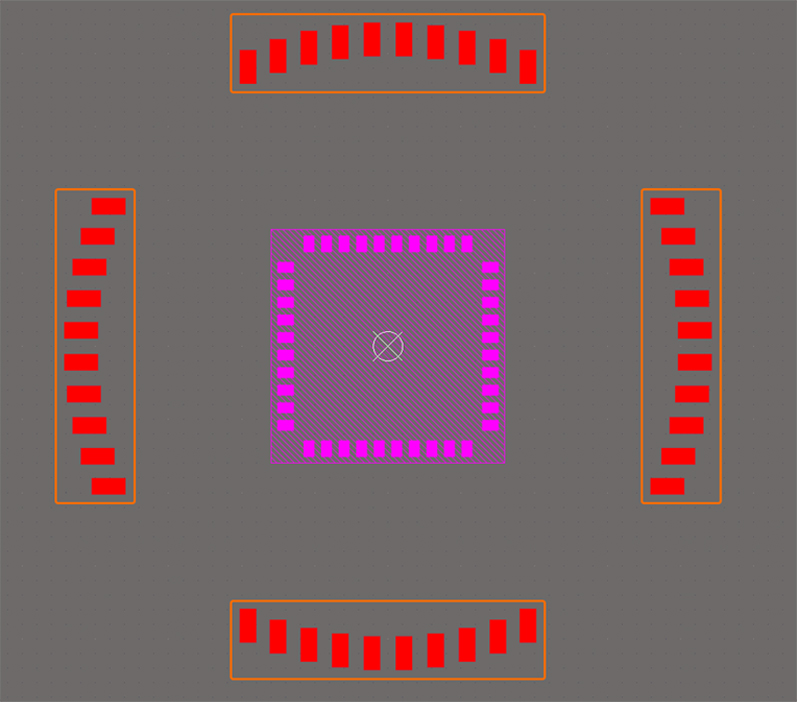
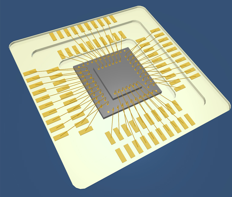
- Maintain Uniform Pad Layout: Arrange pads in straight lines or circular patterns for easier alignment during bonding. Avoid irregular shapes or misaligned pads, as these increase the risk of bonding errors and wire misplacement.
- Ensure Precise Solder Mask Openings: All pads must be fully exposed with solder mask openings slightly larger than the pad itself. This prevents solder mask contamination while avoiding excessive exposure that weakens the PCB structure.
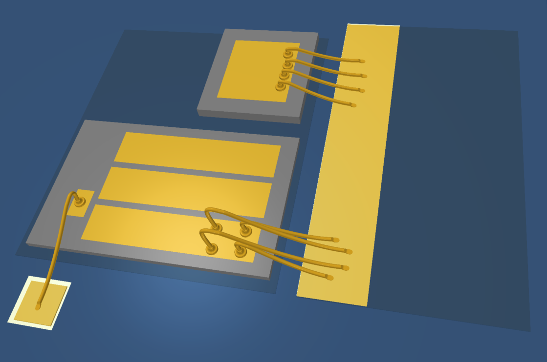
- Keep Pad Surfaces Clean and Flat: Do not place vias or traces on the pad surface, as these create unevenness that disrupts bond formation and reduces mechanical strength.
- Align Pads with Chip Bond Pads: Ensure pads are aligned with the chip’s bond pads to minimize wire length and loop height, which reduces parasitic inductance and improves signal integrity.
- Verify Pad Count and Position: Cross-check pad count and position against the chip’s specifications to ensure one-to-one correspondence, avoiding mismatches that lead to bonding failures.
What Material Is Used for Wire Bonding Pads?
Wire bonding pad materials are selected based on bonding process compatibility, electrical conductivity, and resistance to oxidation and metal diffusion. Key materials and their characteristics are as follows:
- Aluminum: The most widely used base material for wire bonding pads, valued for its excellent bondability with both gold and aluminum bonding wires. It features low cost and good compatibility with mainstream bonding processes, making it suitable for most general-purpose semiconductor and PCB applications.
- Aluminum-Copper Alloys: An upgraded version of pure aluminum, typically containing 1-2% copper. It enhances mechanical strength and electromigration resistance compared to pure aluminum, making it ideal for high-power, high-reliability scenarios such as automotive electronics and industrial control devices.
- Copper: Preferred for high-frequency and advanced process designs, thanks to its superior electrical conductivity and thermal performance. It enables better signal transmission and heat dissipation, but requires additional surface treatment (such as ENIG) to prevent oxidation, which would otherwise compromise bond quality.
- Titanium-Tungsten (TiW): A common barrier layer material, used to prevent metal diffusion between the pad and internal circuitry. It avoids the formation of brittle intermetallic compounds that can cause bond failure, ensuring long-term structural stability of the pad.
- Titanium Nitride (TiN) / Tantalum Nitride (TaN): Alternative barrier layer materials, offering excellent corrosion resistance and diffusion barrier performance. They are often used in high-reliability and high-frequency designs to further enhance pad durability.
- Titanium / Chromium: Mainly used as adhesion layers, ensuring strong bonding between the wire bonding pad and the PCB’s passivation layer or semiconductor substrate. They eliminate the risk of pad detachment, improving the overall reliability of the interconnect structure.
What Is the Appropriate Size of Wire Bonding Pad Design for Different Bonding Processes?
Wire bonding pad size varies by bonding process, wire diameter, and equipment capabilities, with standardized dimensions to ensure consistent bond formation. For ball bonding, the most common process for high-volume manufacturing, pad size is determined by the wire diameter and ball size, which is in line with IPC standards that recommend pad sizes proportional to wire/ball dimensions.
Gold wire ball bonding (most widely used for general-purpose bonding):
- 0.8-1.0 mil wire diameter: Recommended pad size: 60-100 μm (diameter or square), ensuring the bond ball can fully adhere to the pad surface without overflow or insufficient contact.
- 1.2-1.5 mil wire diameter: Pad size increases to 100-150 μm to accommodate the larger bond ball, following the principle that pad size should be 1.5-2 times the wire diameter for reliable bonding.
Copper wire ball bonding (for high-conductivity, high-reliability scenarios):
Requires slightly larger pads than gold wire bonding, typically 70-120 μm for 0.8-1.0 mil wires, due to copper’s higher hardness and different bond formation characteristics, which demand a larger contact area for stable bonding.
Wedge bonding (commonly used for aluminum wires and fine-pitch scenarios, critical for tight-spacing designs):
- 1.0 mil aluminum wedge bonding: Minimum pad size: 60 μm (wide) × 90 μm (tall); suggested size: 120 μm × 120 μm for improved manufacturability, ensuring alignment accuracy and reducing bonding defects during SMT processing.
- Fine-pitch wedge bonding (≤50 μm pitch): Usessmaller pads, down to 40 μm in width, but requires tighter tolerance control to maintain reliability, which is essential for HDI boards and fine-pitch ICs with narrow pad spacing.
How to Determine the Spacing of Wire Bonding Pad Design to Ensure Reliability?
Key determinants of wire bonding pad spacing: wire diameter, bond ball size, loop height, and wire-to-wire shorting risk. Minimum spacing must prevent wire contact, accounting for loop height variations and manufacturing tolerances.
Ball bonding spacing:
- Minimum center-to-center spacing: Typically 1.5 times the pad size; at least 50 μm for fine-pitch designs. Example: 100 μm pads require 150 μm minimum spacing to avoid wire crossover/shorting.
Wedge bonding spacing:
- Critical due to directional bonding: 50 μm minimum for standard scenarios; 30-40 μm for fine-pitch (smaller wires).
- Loop height consideration: Ranges 150-250 μm for most scenarios; overly close pads increase loop contact risk, especially under thermal cycling/mechanical stress.
Key requirement: Consult bonding equipment specifications for minimum spacing; add 10-20% buffer to offset manufacturing variations and alignment errors.
What Are the Considerations for Wire Bonding Pad Design in High-Frequency Scenarios?
Wire bonding pad design for high-frequency scenarios focuses on minimizing parasitic inductance and capacitance, maintaining impedance matching, and reducing signal loss. Key considerations are as follows:
- Optimize Pad Size and Shape: Use smaller, compact pads tailored to the wire diameter and bonding process to reduce parasitic capacitance (larger pads act as capacitors, degrading high-frequency performance). Ensure pad edges are smooth to avoid signal scattering and reflections caused by irregular shapes.
- Minimize Wire Length: Place pads as close as possible to the signal source to reduce wire length, which directly lowers parasitic inductance, it is critical for preserving signal integrity at high frequencies.
- Select High-Performance Materials: Prioritize copper pads over aluminum, as copper offers lower resistance and better thermal conductivity, facilitating efficient signal transmission and heat dissipation (high-frequency signals generate more heat).
- Adopt Suitable Surface Treatments: Use surface treatments that reduce contact resistance (e.g., thin gold plating) to improve signal transmission, ensuring stable electrical contact even at high frequencies.
- Maintain Consistent Pad Spacing: Ensure uniform pad spacing to preserve uniform impedance across all interconnects, preventing signal distortion and maintaining consistent high-frequency performance.
How to Avoid Common Mistakes in Wire Bonding Pad Design?
Avoiding common mistakes in wire bonding pad design requires strict adherence to process rules, thorough validation, and attention to detail. The most frequent mistake is ignoring manufacturer design rules, which leads to pads that are too small, spaced too closely, or improperly aligned with bonding equipment.
- Never use non-standard pad sizes or shapes without verifying compatibility with the bonding process. Always reference the equipment’s design rule document for minimum dimensions and spacing.
- Avoid placing vias, traces, or solder mask over the pad surface, as these create unevenness and disrupt bond formation. Solder mask openings must be precise, neither too small (which covers part of the pad) nor too large (which weakens the PCB).
- Do not misalign pads with the chip’s bond pads, as this increases wire length and loop height, leading to higher inductance and reduced reliability. Always cross-verify pad positions against the chip’s datasheet.
- Avoid inconsistent pad spacing or layout, which complicates bonding alignment and increases the risk of wire crossover. Maintain uniform spacing and arrange pads in regular patterns.
- Do not skip surface treatment or use improper materials, as this leads to poor bond adhesion, oxidation, and premature failure. Select surface treatments compatible with the bonding wire and process.
What Surface Treatment Is Required for Wire Bonding Pad Design?
Wire bonding pad surface treatment is essential to improve bond adhesion, prevent oxidation, and ensure consistent electrical contact. The choice of treatment depends on the pad material, bonding wire type, and scenario requirements, with specific treatments detailed below:
- Aluminum Pads (General Scenarios): The most common surface treatment is chemical nickel gold (ENIG), which provides a thin, uniform gold layer (0.05-0.1 μm) over a nickel barrier. ENIG prevents aluminum oxidation, improves bondability with gold and copper wires, and offers excellent corrosion resistance.
- Aluminum Pads (High-Reliability Scenarios): Use ENIG with a thicker gold layer (0.2-0.3 μm) to enhance bond strength, suitable for high-power, high-reliability applications like automotive electronics.
- Copper Pads (Standard Treatment): Adopt ENIG, where the nickel layer acts as a barrier between copper and gold, effectively preventing copper oxidation and ensuring stable bond adhesion.
- Copper Pads (Low-Cost Scenarios): Use immersion gold (IG) as an alternative. It is more cost-effective than ENIG but offers thinner gold layers and lower corrosion resistance, suitable for non-critical applications.
- Aluminum Pads for Aluminum Wire Bonding: No additional surface treatment is needed, but the pad surface must be clean and free of oxides, contaminants, or scratches. A thin oxide layer can be removed via plasma cleaning before bonding to improve adhesion.
How Does Wire Bonding Pad Design Affect Bonding Quality and Yield?
Wire bonding pad design directly impacts bonding quality and yield by influencing bond strength, alignment accuracy, and resistance to environmental stress. Poorly designed pads lead to frequent bond failures, misaligned wires, and increased manufacturing defects, reducing yield and increasing costs.
Key impacts of pad design:
- Pad size too small: Results in weak bonds that fail during pull testing.
- Oversized pads: Increases material costs and parasitic capacitance.
- Improper spacing: Causes wire-to-wire shorting or crossover, leading to electrical failures.
- Uneven pad surfaces: Results in inconsistent bond formation and reduced mechanical strength.
- Surface treatment issues: Leads to poor bond adhesion and premature failure under thermal cycling or humidity.
Properly designed pads, with correct size, spacing, surface treatment, and layout, ensure consistent bond formation, reduce defects, and improve yield. Well-designed pads also enhance long-term reliability, reducing field failures and warranty costs.
What Are the Differences in Wire Bonding Pad Design for Ball Bonding and Wedge Bonding?
| Design Characteristics | Ball Bonding | Wedge Bonding |
|---|---|---|
| Pad Shape | Round or square, to accommodate the spherical bond | Rectangular, to match the wedge tool’s shape |
| Pad Size | Larger relative to wire diameter (typical ratio 1.5:1) | Minimum 60 μm wide by 90 μm tall (standard); 40×80 μm (fine-pitch) |
| Pad Arrangement | Any pattern, less direction-sensitive | Straight line with consistent spacing, more direction-sensitive |
| Surface Treatment | Commonly ENIG, to improve bondability with gold/copper wires | No additional treatment for aluminum pads (only cleaning required) |
| Fine-Pitch Compatibility | Minimum pitch 50 μm | Better for fine-pitch (down to 30 μm), requires tighter spacing control |
| Solder Mask Openings | Standard openings, no special requirements | Slightly larger openings to accommodate directional bond formation |
Wire Bonding Pad Design Parameter Table: Standard Specifications and Reference Values
| Bonding Process | Wire Diameter (mil) | Pad Size (μm) | Minimum Pad Spacing (μm) | Surface Treatment | Recommended Pad Shape |
| Gold Ball Bonding | 0.8-1.0 | 60-100 | 100 | ENIG (0.05-0.1 μm gold) | Square/Circular |
| Gold Ball Bonding | 1.2-1.5 | 100-150 | 150 | ENIG (0.1-0.2 μm gold) | Square/Circular |
| Copper Ball Bonding | 0.8-1.0 | 70-120 | 120 | ENIG/IG | Square |
| Aluminum Wedge Bonding | 1.0 | 60×90 (min), 120×120 (suggested) | 50 | None (clean aluminum) | Rectangular |
| Fine-Pitch Wedge Bonding | 0.5-0.8 | 40×80 | 30-40 | ENIG (for copper pads) | Rectangular |
How to Optimize Wire Bonding Pad Design for Cost and Performance Balance
Optimizing wire bonding pad design for cost and performance balance focuses on avoiding over-engineering, matching design to actual scenario requirements, and reducing unnecessary costs while ensuring basic reliability and performance. Specific optimization measures are detailed below:
- Adopt Standard Pad Sizes and Shapes: Prioritize standard sizes and shapes (e.g., square/circular for ball bonding, rectangular for wedge bonding) instead of custom designs. Custom pad sizes require specialized manufacturing processes and additional tooling, which significantly increase production costs. Standard designs also improve compatibility with mainstream bonding equipment.
- Select Materials Based on Scenario Requirements: For low-power, non-critical applications (e.g., general consumer electronics), use aluminum pads with no additional surface treatment. They are low-cost and meet basic bonding needs. Reserve copper pads (with higher cost and better performance) for high-frequency, high-power, or high-reliability scenarios (e.g., automotive electronics, industrial controls).
- Optimize Pad Size to Reduce Material Waste: Minimize pad size to the minimum requirement specified by the bonding process and wire diameter. Avoid oversized pads, as they waste conductive materials (aluminum/copper) and increase material costs. Ensure the reduced size still meets bond strength and alignment requirements to avoid performance issues.
- Choose Cost-Effective Surface Treatments: For non-critical, low-humidity scenarios where corrosion resistance is not a priority, use immersion gold (IG) instead of the more expensive chemical nickel gold (ENIG). IG reduces costs while still providing basic bond adhesion, and ENIG should be reserved for high-reliability or harsh-environment applications.
- Collaborate with Manufacturers Early: Engage with bonding equipment manufacturers and PCB fabricators in the early design stage. They can provide professional advice on cost-saving opportunities (e.g., compatible standard parameters, material alternatives) without compromising pad reliability and performance, which helps avoid costly design modifications later.
What Testing Methods Are Used to Verify the Rationality of Wire Bonding Pad Design
Several testing methods verify the rationality of wire bonding pad design, ensuring it meets mechanical, electrical, and reliability requirements. These tests validate bond strength, electrical performance, and resistance to environmental stress. Below are common testing methods:
- Wire pull testing: Measures the force required to pull a bonded wire from the pad. Evaluates bond strength and identifies weak bonds caused by improper pad size, surface treatment, or layout. Follows international standards with minimum pull force requirements based on wire diameter and pad material.
- Shear testing: Measures the force required to shear the bond from the pad surface. Evaluates the bond’s mechanical integrity, particularly useful for verifying wedge bond quality and pad surface flatness.
- Electrical testing: Includes resistance measurement to ensure low contact resistance, and signal integrity testing to verify impedance matching and parasitic effects (critical for high-frequency designs).
- Thermal cycling testing: Exposes pads to extreme temperature changes to evaluate resistance to thermal stress, identifying failures from material mismatches or poor design.
- Microscopic inspection: Examines pad surface quality, bond alignment, and intermetallic compound formation, ensuring no defects that could impact performance.
FAQs About Wire Bonding Pad Design
Q1: What happens if wire bonding pad size is smaller than the recommended minimum?
A1: Pads smaller than the recommended minimum lead to weak bonds that fail during pull or shear testing. The bond ball or wedge cannot fully adhere to the pad, reducing mechanical strength and increasing the risk of bond separation under thermal cycling or mechanical stress. This also increases manufacturing defects and reduces yield, as bonds are more likely to misalign or fail during the bonding process.
Q2: Can the same wire bonding pad design be used for both gold and aluminum wires?
A2: No, the same design cannot be used for both gold and aluminum wires. Gold wires require pads with surface treatments like ENIG to prevent oxidation and improve bond adhesion, while aluminum wires can bond directly to clean aluminum pads without additional treatment. Pad size also differs slightly, with gold wire ball bonding requiring larger pads relative to wire diameter compared to aluminum wire wedge bonding.
Q3: How does pad surface roughness affect wire bonding pad design performance?
A3: Excessive surface roughness disrupts bond formation, leading to inconsistent bond strength and poor electrical contact. Rough surfaces create gaps between the wire and pad, reducing adhesion and increasing contact resistance. Pad surfaces must be smooth and free of scratches, dents, or contaminants to ensure uniform bond formation and reliable electrical connectivity.
Q4: What is the minimum solder mask opening size for wire bonding pads?
A4: The minimum solder mask opening size is typically 10-20 μm larger than the pad size on all sides. This ensures the pad is fully exposed without solder mask contamination, while preventing excessive exposure that weakens the PCB structure. For example, a 100 μm pad requires a solder mask opening of 120-140 μm to ensure proper exposure.
Q5: How to adjust wire bonding pad design for fine-pitch bonding processes?
A5: For fine-pitch bonding, reduce pad size and spacing while maintaining strict tolerance control. Use rectangular pads for wedge bonding or small square pads for ball bonding, with minimum pad sizes down to 40 μm. Increase alignment precision to ensure pads are properly positioned relative to the chip’s bond pads, and use surface treatments that improve bondability with smaller wires. Consult the bonding equipment’s design rules for specific fine-pitch requirements.
Q6: Does wire bonding pad design affect thermal performance?
A6: Yes, wire bonding pad design impacts thermal performance. Larger pads with higher thermal conductivity materials such as copper dissipate heat more effectively, reducing thermal stress on the bond and improving long-term reliability. Proper pad spacing also allows for better heat distribution, preventing hotspots that can degrade bond quality. For high-power scenarios, larger pads and thermal vias near the pad can enhance heat dissipation.
You may also like


Tags: Wire Bonding Pad Design, Wire Bonding Pad Design Guideline, Wire Bonding Pad Design Parameter, Wire Bonding Pad Design Rules