

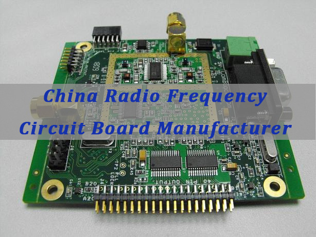
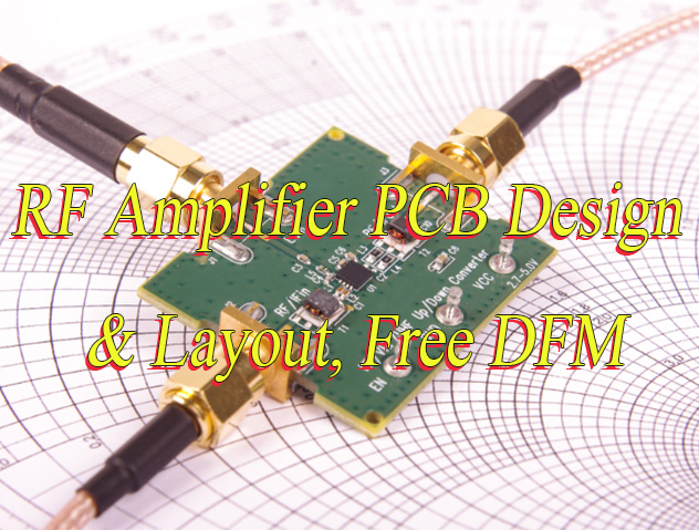
China radio frequency circuit board manufacturer capabilities are becoming increasingly important as modern electronics move toward higher operating frequencies. This article explains how RF circuit boards support technologies such as 5G infrastructure, satellite communication, automotive radar, and IoT devices, while outlining the materials, design considerations, and manufacturing processes required to achieve stable high-frequency performance.
EBest Circuit (Best Technology) is an experienced China radio frequency circuit board manufacturer specializing in high-frequency PCB fabrication for advanced wireless applications. Our engineering team provides constructive DFM feedback to ensure RF layouts remain coherent with signal integrity requirements and manufacturing feasibility. We support Rogers, PTFE, and other high-frequency laminates to build circuit boards fully compatible with demanding RF system architectures. Meanwhile, our structured production management includes contingency planning to ensure stable delivery schedules and reliable quality throughout prototyping and production stages. If you are evaluating a dependable RF PCB manufacturing partner, we would be pleased to discuss your project requirements. For RF PCB fabrication, prototyping, or assembly support, please feel free to contact us at sales@bestpcbs.com.
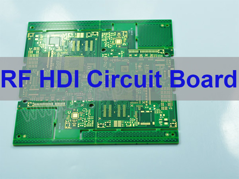
What Is a Radio Frequency Circuit Board?
A radio frequency circuit board (RF PCB) is a printed circuit board specifically engineered to transmit and process signals operating in the radio frequency range, typically from several hundred megahertz to multiple gigahertz. Unlike standard digital PCBs, RF circuit boards must maintain signal integrity under high-frequency conditions where electromagnetic effects become significant.
RF PCBs are commonly used in systems such as wireless communication modules, satellite electronics, radar equipment, and high-speed networking hardware. To achieve stable performance, these boards rely on materials with low dielectric loss and precisely controlled impedance structures.
Several factors distinguish RF PCBs from conventional boards:
| Feature | RF PCB | Standard PCB |
|---|---|---|
| Material | Rogers, PTFE, Taconic | FR4 |
| Frequency range | MHz to GHz | Mostly below 1 GHz |
| Signal loss | Very low | Moderate |
| Design complexity | High | Standard |
Because high-frequency signals are extremely sensitive to trace geometry and material properties, RF PCB design requires careful engineering analysis and simulation before manufacturing begins.
Why Choose China Radio Frequency Circuit Board Manufacturers?
Over the past two decades, China has become one of the most important global manufacturing centers for high-frequency printed circuit boards. Many international electronics companies source RF PCB fabrication in China due to a combination of advanced capabilities and competitive production environments.
Several factors make Chinese RF PCB suppliers attractive to international customers.
Cost efficiency through manufacturing scale
China’s electronics manufacturing ecosystem enables large-scale PCB production while maintaining competitive pricing. Material sourcing, fabrication, and assembly services are often vertically integrated, reducing overall production costs.
Mature high-frequency PCB manufacturing capability
Experienced Chinese PCB factories support a wide range of high-frequency materials, including:
- Rogers laminates
- PTFE-based substrates
- Taconic high-frequency materials
- Ceramic RF substrates
These materials enable the production of microwave circuit boards used in demanding applications such as radar and communication infrastructure.
Integrated PCB and PCBA services
Many RF PCB manufacturers in China offer full turnkey services including PCB fabrication, component sourcing, and PCBA assembly. This integration simplifies supply chain management and shortens production cycles.
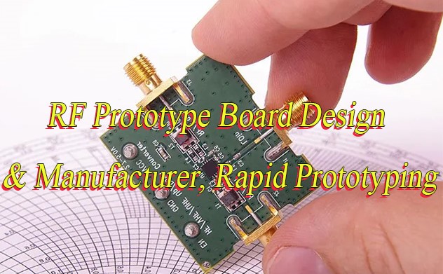
Rapid prototyping capability
Engineering teams developing wireless devices often require quick prototype iterations. China-based PCB manufacturers can typically deliver RF PCB prototypes faster than many regional suppliers.
What Materials Are Used in RF Circuit Boards?
Material selection plays a critical role in RF PCB performance. High-frequency signals are strongly affected by dielectric properties, loss tangent, and thermal stability. As a result, RF PCBs rarely use standard FR4 materials when operating at higher frequencies.
Several specialized substrates are widely used in RF circuit board fabrication.
| Material | Key Characteristics | Typical Applications |
|---|---|---|
| Rogers RO4350B | Low dielectric loss, stable Dk | RF communication systems |
| PTFE laminates | Ultra-low loss, excellent high-frequency performance | Microwave circuits |
| Taconic materials | High reliability in RF environments | Satellite electronics |
| Ceramic substrates | Excellent thermal conductivity | High-power RF systems |
Among these materials, Rogers laminates are particularly popular in RF PCB manufacturing because they offer stable dielectric properties across a wide frequency range.
Material selection directly influences signal attenuation, impedance stability, and thermal management. Therefore, RF PCB design engineers must carefully evaluate substrate characteristics during the early stages of circuit design.
What Frequencies Do RF Circuit Boards Typically Support?
RF circuit boards are designed to operate across a wide range of frequencies depending on their intended applications. Modern RF systems often operate from hundreds of megahertz up to tens of gigahertz.
Common RF frequency ranges include:
| Frequency Range | Typical Applications |
|---|---|
| 2.4 GHz | WiFi, Bluetooth, IoT devices |
| 5 GHz | Wireless networking systems |
| 10 GHz | Radar and microwave communication |
| 24 GHz | Automotive radar |
| 30+ GHz | Millimeter-wave communication |
For example, a 2.4 GHz RF PCB used in wireless modules must maintain extremely consistent impedance characteristics to prevent signal reflection and transmission loss. Even minor variations in trace width or dielectric thickness can affect system performance.
Because of these requirements, RF PCB manufacturing demands highly accurate fabrication processes and controlled material handling.
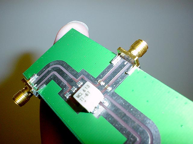
What Are the Key Design Challenges in RF PCB?
Designing RF circuit boards involves challenges that are rarely encountered in conventional PCB design. At high frequencies, electrical behavior becomes heavily influenced by electromagnetic effects.
Impedance control
RF transmission lines must maintain a consistent impedance—typically 50 ohms—to ensure efficient signal transmission. Any deviation can cause reflections and degrade signal quality.
Signal loss
Dielectric loss and conductor loss increase as signal frequency rises. Designers must select materials with low loss tangent to minimize attenuation.
Crosstalk and interference
High-frequency signals can couple into nearby traces, creating unwanted interference. Proper trace spacing and ground plane design are essential to prevent this issue.
Trace geometry
RF traces are often designed using transmission line structures such as microstrip or coplanar waveguide configurations. These structures ensure predictable signal propagation.
Addressing these challenges requires both electromagnetic simulation and practical fabrication experience.
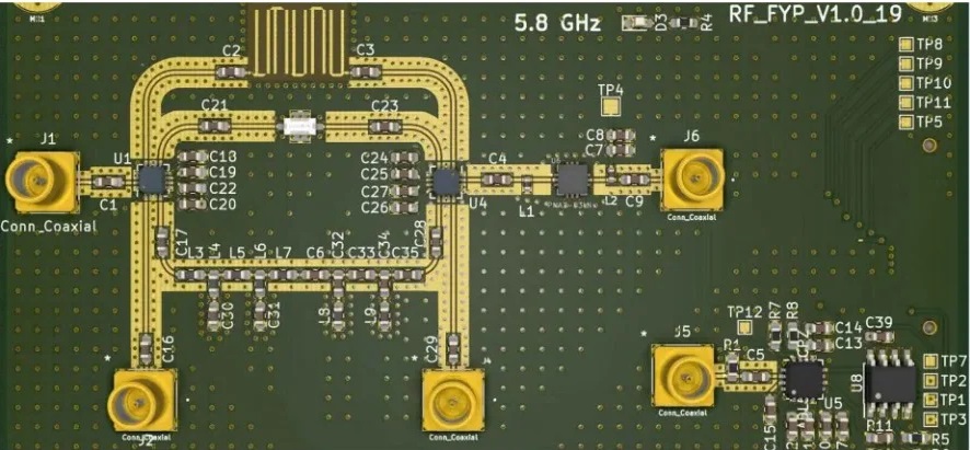
How Does RF PCB Stackup Affect Signal Performance?
The stackup structure of an RF PCB significantly affects signal integrity and electromagnetic behavior. Proper layer configuration helps maintain controlled impedance and reduces electromagnetic interference.
A typical RF PCB stackup might include:
| Layer | Function |
|---|---|
| Top layer | RF signal routing |
| Ground plane | Reference plane for impedance control |
| Inner layers | Power distribution and additional signals |
| Bottom layer | Secondary signal routing |
A well-designed stackup provides stable reference planes and consistent dielectric thickness. This structure enables predictable transmission line behavior and helps minimize signal distortion.
Ground planes also play a crucial role in suppressing electromagnetic noise and stabilizing signal return paths.
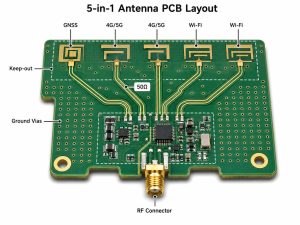
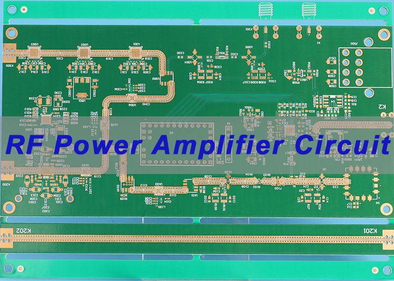
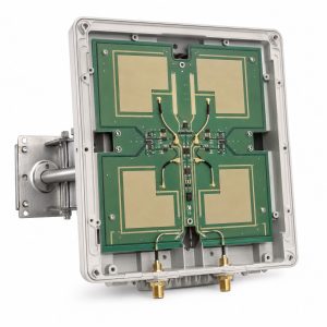
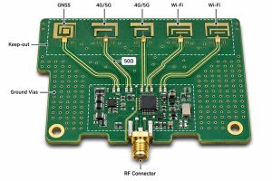
Applications of Radio Frequency Circuit Boards
RF circuit boards support a wide variety of modern electronic systems that rely on wireless communication and high-frequency signal processing.
Wireless communication devices
Smartphones, WiFi routers, and IoT modules all rely on RF PCBs to transmit and receive wireless signals.
5G infrastructure
Base stations and high-speed communication equipment use high-frequency PCBs capable of supporting advanced modulation technologies.
Radar systems
Automotive radar and military radar systems depend on microwave circuit boards for accurate signal processing.
Satellite electronics
Satellite communication equipment requires RF PCBs with extremely low signal loss and stable performance under harsh environmental conditions.
IoT devices
Compact wireless modules used in smart homes and industrial IoT devices frequently integrate RF antenna PCB designs.
These diverse applications illustrate the growing importance of reliable RF PCB manufacturing capabilities.
RF PCB vs Standard FR4 PCB: What Is the Difference?
Although both RF PCBs and conventional PCBs share the same basic manufacturing principles, their performance characteristics differ significantly.
| Parameter | RF PCB | FR4 PCB |
|---|---|---|
| Operating frequency | GHz range | Usually below 1 GHz |
| Dielectric loss | Very low | Higher |
| Material cost | Higher | Lower |
| Typical applications | RF communication, radar | General electronics |
FR4 remains suitable for most digital circuits, but high-frequency systems require materials with lower signal loss and more stable dielectric properties.
What Manufacturing Capabilities Are Required for RF PCB Fabrication?
Producing high-quality RF circuit boards requires advanced manufacturing processes and strict process control. High-frequency PCB fabrication typically involves several specialized capabilities.
Precision drilling and routing
Trace geometry must remain extremely consistent. Even small dimensional deviations can change impedance characteristics.
Controlled lamination
Lamination parameters must be carefully controlled to maintain stable dielectric thickness and prevent material deformation.
Impedance testing
Manufacturers perform impedance verification during production to ensure transmission line performance matches design specifications.
Advanced inspection systems
Techniques such as automated optical inspection and X-ray inspection help detect manufacturing defects that could affect RF performance.
These capabilities are essential for producing reliable high-frequency circuit boards.
How China RF PCB Manufacturers Control Quality?
Quality control is a critical aspect of RF PCB production. Because high-frequency circuits are sensitive to small variations, manufacturers must implement strict inspection and testing procedures.
Typical RF PCB quality control processes include:
- Incoming material inspection to verify substrate properties
- Automated optical inspection to detect trace defects
- Impedance testing to confirm electrical performance
- X-ray inspection for multilayer structure verification
Many experienced Chinese RF PCB manufacturers also operate under international quality certifications such as ISO standards, ensuring consistent production quality for global customers.
How to Choose a Reliable China Radio Frequency Circuit Board Supplier?
Selecting the right RF PCB supplier can significantly influence product performance and long-term reliability. Engineers and procurement teams should evaluate several factors when choosing a manufacturing partner.
Experience with high-frequency materials
A qualified supplier should have extensive experience working with Rogers, PTFE, and other RF substrates.
Impedance control capability
Manufacturers must demonstrate proven impedance control processes and testing capability.
Prototyping and engineering support
Fast prototype turnaround and design assistance can accelerate product development cycles.
Integrated manufacturing services
Suppliers offering PCB fabrication, component sourcing, and PCBA assembly provide greater convenience and supply chain efficiency.
Overall, working with an experienced RF PCB manufacturer helps reduce development risks and improve product reliability.
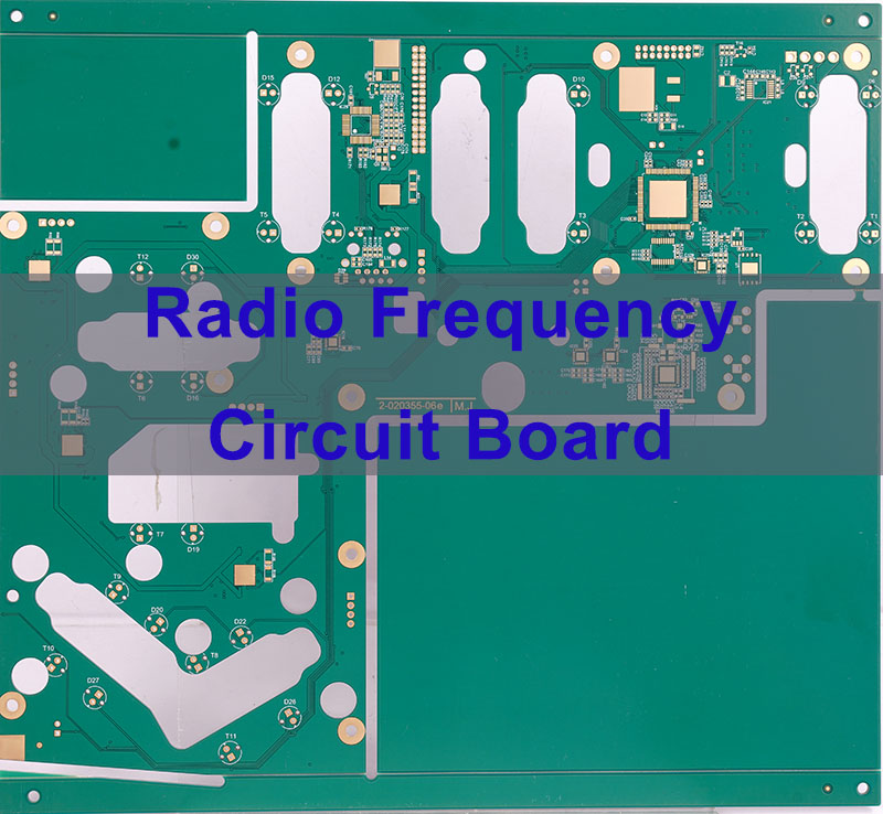
Radio frequency circuit boards play a vital role in modern wireless communication systems, radar technology, satellite electronics, and high-speed networking equipment. Their design and manufacturing require specialized materials, precise impedance control, and highly controlled fabrication processes.
For companies developing high-frequency electronics, partnering with an experienced RF PCB manufacturer ensures stable signal performance and reliable product operation.
If you are looking for a professional China radio frequency circuit board manufacturer capable of RF PCB fabrication, prototyping, and assembly services, feel free to contact us at sales@bestpcbs.com.
FAQs about China Radio Frequency Circuit Boards
What materials are commonly used in RF PCBs?
RF circuit boards typically use specialized substrates such as Rogers laminates, PTFE materials, Taconic laminates, and ceramic substrates. These materials provide low dielectric loss and stable electrical performance at high frequencies.
Why are Rogers materials widely used in RF PCB design?
Rogers laminates offer stable dielectric constants and low loss characteristics, making them suitable for microwave and high-frequency circuit applications.
What frequencies can RF PCBs support?
RF circuit boards can support frequencies ranging from several hundred megahertz to more than 30 GHz, depending on the substrate material and circuit design.
How much does RF PCB fabrication cost?
The cost of RF PCB fabrication depends on factors such as material type, layer count, board size, and production volume. High-frequency materials typically increase the overall manufacturing cost.
How long does RF PCB manufacturing take?
RF PCB manufacturing lead time depends on several factors, including material availability, layer count, impedance requirements, and overall fabrication complexity. Prototype RF PCBs can often be completed within several days for simple structures, while multilayer high-frequency boards typically require more processing time due to specialized materials and tighter tolerance control.
At EBest Circuit (Best Technology), our optimized production workflow enables most RF PCB projects to be completed within approximately 1.5 weeks, covering fabrication and basic preparation for assembly. This balanced schedule allows sufficient process control for high-frequency materials while still supporting efficient product development cycles.
You may also like
Tags: China Radio Frequency Circuit Board, China Radio Frequency Circuit Board Manufacturer, China RF PCB manufacturer, China RF PCB supplier, rf pcb fabrication china, rf pcb manufacturer china