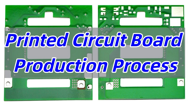
The printed circuit board production process is the fundamental sequence of steps that brings electronic designs to life. Understanding this process is key to appreciating the engineering behind the devices we use daily. This article will walk you through each stage, explain the importance of materials, and show how quality is guaranteed from start to finish.
Have you ever wondered what separates a high-performance, reliable PCB from one that fails prematurely? Are you struggling with:
- Inconsistent quality from one production batch to the next?
- Confusing communication and a lack of technical support from your supplier?
- Delays in delivery that disrupt your own production schedules?
- Hidden costs that appear after you’ve placed an order?
- Limited capabilities in a supplier, preventing you from exploring advanced designs?
At EBest Circuit (Best Technology), we’ve built our entire operation around solving these exact problems. We provide:
- A rigorous, data-driven quality control system that ensures every board, every time, meets spec.
- Direct access to experienced engineers who speak your language and understand your challenges.
- A streamlined production flow managed by advanced MES and ERP systems for on-time delivery.
- Upfront, transparent pricing with no surprises, allowing for accurate budgeting.
- A one-stop solution from basic FR4 boards to complex HDI, flex, and rigid-flex PCBs.
EBest Circuit (Best Technology) is a specialized PCB manufacturer with a modern, highly automated facility in China. Our team of seasoned engineers leverages cutting-edge technology to deliver great quality boards. We pride ourselves on being a reliable extension of your engineering team. For a consultation on your next project, reach out to us at sales@bestpcbs.com.
What Is the Printed Circuit Board Production Process?
The printed circuit board production process is the methodical series of steps used to manufacture the essential electrical pathways that connect components in electronic devices.
At its core, the process is about creating order out of raw materials. It involves precisely patterning conductive pathways onto insulating substrates, connecting multiple layers with microscopic precision, and protecting the circuit from environmental challenges. Understanding this flow is crucial for any engineer or purchaser, as it highlights the critical control points that separate a good board from a great one.
At EBest Circuit (Best Technology), we see this process as our core expertise, not just a series of steps. Our approach is built on a foundation of three key principles:
- Precision Engineering: We go beyond basic specifications. For instance, our drilling capabilities can achieve hole diameters as small as 0.1mm with positional accuracy of ±0.025mm, ensuring perfect alignment for even the most dense designs.
- Controlled Automation: Our factory floor features fully automated optical inspection (AOI) systems that scan every layer for defects invisible to the human eye. This isn’t just about efficiency; it’s about eliminating human error and guaranteeing consistency across every production panel, from the first board to the thousandth.
- Proactive Collaboration: The process starts long before production. Our engineering team conducts a thorough Design for Manufacturability (DFM) analysis on every order. We don’t just build your design; we partner with you to identify potential issues like acid traps or insufficient copper balancing upfront, saving time and cost by preventing failures before they happen.
This meticulous attention to detail at every stage—from material selection and chemical processing to final electrical testing—is what defines our printed circuit board fabrication process flow. It’s how we ensure that every board leaving our facility not only meets the print but is built to exceed expectations, fully embodying our commitment to quality that is “Made in China, Trusted Worldwide.”
Printed Circuit Board Production Process – EBest Circuit (Best Technology)
At EBest Circuit (Best Technology), we understand that high-frequency PCB manufacturing requires specialized expertise. While standard FR-4 boards follow conventional workflows, PTFE-based high-frequency materials demand precise process adaptations. Here’s how we handle different high-frequency board scenarios:
A. NPTH PTFE Boards: Streamlined for Simplicity
For non-plated-through-hole PTFE applications, we employ an optimized process:
- Panel Preparation: Precision cutting of PTFE laminates
- Drilling: Creating component holes with PTFE-optimized parameters
- Circuit Patterning: Direct imaging and pattern transfer
- Etching: Precise copper removal to define circuits
- AOI Inspection: Automated optical verification
- Solder Mask Application: Protection with high-frequency compatible materials
- Legend Printing: Component identification markings
- Board Profiling: CNC routing to final dimensions
- Electrical Testing: Continuity and performance verification
- Final QC: Comprehensive quality checks
- Surface Finish: Immersion tin application
- Pre-shipment Verification: Final quality assurance
- Packaging & Shipping: Secure delivery with certification
B. PTH PTFE Boards: Two Proven Methodologies
Negative Pattern Process (Preferred for High-Frequency):
- Material preparation with optimized panel sizes
- Precision drilling with PTFE-specific parameters
- Plasma treatment for superior hole wall preparation
- Electroless copper deposition for initial conductivity
- Full-thickness panel plating in single operation
- Circuit pattern imaging and development
- Comprehensive inspection protocols
- Acidic etching for precise circuit definition
- Post-etch verification and measurement
- Solder mask application
- Legend printing
- Board separation and profiling
- Electrical testing including impedance control
- Final quality inspection
- Surface finishing
- Pre-shipment quality confirmation
- Secure packaging and documentation
Positive Pattern Process:
- Follows similar initial steps through panel plating
- Pattern plating for selective copper thickening
- Alkaline etching process
- Enhanced inspection protocols
- Continued through standard finishing steps
C. Multilayer PTFE & Hybrid Constructions
For complex multilayer boards:
- Inner Layer Processing: Sequential lamination preparation
- Baking Protocol: 30-minute baking at 120°C after browning
- Layer Alignment: Precision registration systems
- Lamination: Controlled pressure and temperature cycles
- PTFE-Specific Drilling: Optimized parameters for material characteristics
- Differentiated Hole Preparation: Plasma treatment for PTFE, alternative methods for non-PTFE materials
- Copper Deposition: Controlled electroless copper application
- Outer Layer Processing: Pattern transfer and plating
- Final Processing: Completion through standard workflow
Key Differentiators for High-Frequency Success:
- Material-Specific Expertise: Each material family receives customized processing parameters
- Process Optimization: Critical adjustments at drilling, plating, solder mask, and routing stages
- Quality Assurance: Enhanced inspection protocols at each manufacturing stage
- Technical Flexibility: Ability to handle pure PTFE, ceramic hydrocarbon, and hybrid constructions
Our manufacturing approach ensures that whether you require simple NPTH designs or complex multilayer high-frequency boards, each product receives the specialized attention necessary for optimal RF performance. The careful process adaptations for PTFE materials—particularly in drilling, hole preparation, and plating stages—make the crucial difference in achieving consistent high-frequency performance.
By maintaining strict process controls and material-specific expertise, we deliver high-frequency PCBs that meet the most demanding performance specifications while ensuring manufacturing reliability and consistency.
Material Matters: Why We Choose the Right Base for Every Application
Think of your PCB’s substrate as the foundation of a building. A weak or unsuitable foundation will compromise the entire structure, no matter how perfect the design. The base material is not just a passive platform; it actively dictates your board’s electrical performance, thermal resilience, mechanical strength, and ultimate reliability. Choosing the wrong material is a primary reason behind field failures, signal integrity issues, and manufacturing defects.
At EBest Circuit (Best Technology), we go beyond simply sourcing laminates from top global suppliers. Our engineering team acts as your guide, translating complex material properties into practical solutions for your specific application. We help you navigate the critical trade-offs between performance, cost, and manufacturability.
1. FR-4
FR-4 remains the industry standard for a vast range of applications due to its excellent balance of properties and cost-effectiveness.
- What It Is: A composite material made from woven fiberglass cloth and an epoxy resin binder.
- Key Considerations: The critical differentiator within FR-4 is its Glass Transition Temperature (Tg). Think of Tg as the temperature at which the solid substrate begins to soften. Standard FR-4 has a Tg around 130-140°C, which is sufficient for conventional soldering processes.
- When to Choose High-Tg FR-4: For lead-free soldering (which requires higher temperatures) or applications in elevated temperature environments (like under-hood automotive electronics), High-Tg FR-4 (≥170°C) is essential. It provides superior thermal stability, preventing board deformation (delamination) and ensuring long-term reliability. We also pay close attention to the Td value (Decomposition Temperature); a higher Td (e.g., >350°C) means better resistance to thermal breakdown during repeated thermal cycles.
2. High-Speed Materials
When your design involves high-frequency signals, standard FR-4 can cause significant signal degradation. This is where specialized high-speed materials come in.
- The Core Parameters: The two most critical properties are Dielectric Constant (Dk or Er) and Dissipation Factor (Df).
- Dk influences the speed of your signals. A stable, low Dk value ensures consistent signal timing and controlled impedance.
- Df measures the signal energy lost as heat. A lower Df (e.g., 0.003 vs. FR-4’s 0.020) is crucial for minimizing loss in high-speed digital applications (like servers, networking gear) and RF circuits.
- Our Approach: We recommend materials like ISOLA’s FR408HR or Panasonic’s Megtron series when signal integrity is paramount. These materials offer tight Dk/Df tolerances and consistency across the panel, which is vital for impedance control.
3. High-Frequency Materials: Engineered for RF & Microwave
For applications pushing into the GHz range (e.g., radar, satellite communications, 5G infrastructure), PTFE-based materials (like Rogers RO4000® series) are the gold standard.
- Why PTFE? These materials exhibit exceptionally low and stable Dk/Df values, enabling minimal signal loss and phase stability at microwave frequencies. However, they require specialized plasma treatment during manufacturing to ensure proper hole wall preparation for reliable plating—a process we have mastered.
- Hybrid Constructions: We expertly manufacture multilayer boards that combine PTFE layers with ceramic-filled hydrocarbon thermoset materials (e.g., RO4350B), optimizing performance and cost.
4. Specialized Substrates for Demanding Applications
- Metal-Core PCBs (Aluminum/Copper): When heat dissipation is the primary concern—such as in high-power LED lighting, power supplies, and automotive modules—metal-core boards are ideal. The metal base acts as an integrated heatsink, efficiently drawing heat away from critical components.
- Flexible Materials (Polyimide): For products that need to bend, fold, or fit into compact spaces (wearables, medical devices, consumer electronics), flexible PCBs made from polyimide offer incredible durability, light weight, and excellent heat resistance.
In summary, understanding how are printed circuit boards made to meet your specific needs starts with selecting the right material. It’s a decision that impacts everything from electrical performance to manufacturing yield. Our engineers are here to demystify the data—from Tg and Td to Dk and Df—and help you select the optimal material that ensures your product’s success without over-engineering the cost.
How EBest Circuit (Best Technology) Ensures Consistent Quality in Every PCB?
Precision in manufacturing is useless without consistent quality. For us, quality is not just a final inspection step. It is a mindset integrated into every stage of our printed circuit board production. We are a precision-focused partner, not just a production shop.
Our commitment is backed by international certifications, including ISO9001, IATF16949 for automotive, ISO13485 for medical, and AS9100D for aerospace. Our inspection methods are robust:
- Automated Optical Inspection (AOI): This system scans the boards to detect common flaws like scratches, stains, or incorrect parts.
- Flying Probe Testing: This is a critical electrical test. It checks for short and open circuits on the bare board, ensuring the netlist matches the design.
- Impedance Control: For high-speed designs, controlling the impedance of traces is vital. We test samples to ensure the impedance values are within your specified tolerance.
- Cross-Section Analysis: We regularly cut sample boards to microscopically inspect the internal layers, plating thickness, and hole wall quality.
This systematic approach eliminates guesswork. It gives you data-driven confidence in the boards you receive.
PCB Assembly Process: From Bare Board to Functional Circuit
EBest Circuit (Best Technology) has our own SMT factories in China and in Vietnam respectively.
Here is our Core Flow of PCB Assembly: Incoming Materials (BGA/PCB) → Baking → Solder Paste → Printing → SPI → Component Placement → Reflow Soldering → Line Clearance → Post-Reflow Inspection → AOI → X-Ray → Through-Hole Insertion (THT) → Cleaning → Programming/Testing → Conformal Coating → Potting → Final Assembly → Labeling → Depaneling → Packaging & Shipping
Detailed Process Breakdown:
- Incoming Materials (BGA/PCB)
- Receipt and verification of customer-supplied PCBs and components (reel, tray, tube, or bulk).
- Initial audit of documentation: BOM, centroid data (pick-and-place coordinates), and solder paste stencil design.
- Baking
- Purpose: To remove moisture absorbed by moisture-sensitive components and PCB substrates, preventing delamination, popcorning, or soldering defects during reflow.
- Specifications:
- All FPCs, sensitive ICs, and LEDs must be baked before production.
- Standard ICs: 120°C for 12 hours.
- LEDs (Tape & Reel): 60°C for 12 hours.
- FPCs / FR-4 PCBs: 120°C for 1.5 hours.
- Storage: Moisture-sensitive materials baked but not used on the same day are stored in controlled dry cabinets.
- Solder Paste Management
- Primary Alloy: We recommend and primarily use high-temperature solder paste.
- Senju (Japanese Brand): Sn96.5%/Ag3.0%/Cu0.5%.
- Alternative Domestic Brand: Sn99%/Ag0.3%/Cu0.7%.
- Handling Protocol:
- Storage: Refrigerated at 2-10°C.
- Thawing: Paste must be thawed for a minimum of 4 hours prior to use.
- Mixing: Paste must be mixed for 3 minutes to ensure homogeneous consistency.
- Note: We advise against low-temperature solder paste due to its inferior wetting properties and lack of silver/copper content.
- Primary Alloy: We recommend and primarily use high-temperature solder paste.
- Solder Paste Printing
- Tooling: Uses laser-cut stencils (framed stainless steel) to deposit paste onto PCB pads.
- Stencil Types: Standard, Step-up/Step-down, and Nano-coated (reduces paste adherence to apertures, improving print quality).
- Common Sizes: 42x52cm (most common), up to 73.6×73.6cm.
- Thickness: Ranges from 0.08mm to 0.15mm, determining solder paste volume. Aperture size is typically 10-20% larger than the pad.
- Stencil Life: A stencil is retired if its tension measures ≤25N/cm² or after approximately 50,000 prints. Client-owned stencils are archived for three years.
- Equipment: High-precision automated printers (e.g., GKG) with accuracy up to ±0.025mm.
- Small PCB Support: PCBs smaller than the printer’s minimum size require a custom carrier fixture.
- Solder Paste Inspection (SPI)
- A 3D optical system inspects the paste printing quality immediately after the printer.
- Measures: Paste volume, area, height, and alignment to detect defects like bridging, insufficient solder, or misplacement. Inspection precision is 10µm.
- Automated Component Placement
- Equipment: 4 SMT lines (2 Juki, 2 Yamaha YSM20R). The Yamaha YSM20R offers high-speed placement of up to 95,000 components per hour with an accuracy of ±0.035mm, supporting 0201 metric chip components.
- Programming Requirements: BOM, centroid data, and board CAD data (for footprint verification).
- Process: Components are picked from feeders using vacuum nozzles and placed with high precision.
- Reflow Soldering
- The PCB passes through a controlled thermal profile to melt the solder paste, forming permanent solder joints.
- Reflow Options:
- Nitrogen (N₂) Reflow: Soldering in an oxygen-free environment results in brighter, more reliable solder joints with significantly reduced oxidation and up to 10% fewer voids. This is our premium quality process.
- Air Reflow: Standard process for many applications.
- Process Control: Thermal profiles are meticulously monitored and recorded using profiling equipment to ensure they meet the specific requirements of the solder paste (e.g., peak temp ~220-245°C for high-temperature paste). Typical cycle time is 7-8 minutes.
- Line Clearance & Post-Reflow Inspection
- Line Clearance: Verification and accounting of all materials used in the production batch.
- Post-Reflow Inspection: Initial manual visual inspection for gross defects like misplaced or tombstoned components, poor solder wetting, or board discoloration.
- Automated Optical Inspection (AOI)
- A high-speed camera system performs a comprehensive 2D/3D inspection of the assembled board.
- Detects: Missing, misaligned, wrong, or damaged components; soldering defects like bridging, insufficient solder, and lifted leads.
- X-Ray Inspection (AXI)
- Purpose: To inspect hidden solder connections, such as those on Ball Grid Arrays (BGAs) and other bottom-termination components.
- Rule: This step is mandatory for assemblies containing BGAs or any components with hidden joints.
- Quality Standard: We adhere to an industry-standard voiding ratio of <25% for general electronics, with <10% achievable for automotive/medical-grade applications.
- Through-Hole Technology (THT) / Manual Assembly
- Process: Insertion and soldering of pin-in-hole components.
- Equipment: Selective soldering machines are used for high-reliability applications, supporting PCBs up to 300x350mm with a placement accuracy of ±0.05mm.
- Tools: ESD-safe soldering stations, solder wire, and appropriate PPE (mask, gloves).
- Cleaning
- Removal of flux residues and other contaminants post-soldering using approved solvents (e.g., alcohol, flux remover) or advanced methods like dry ice blasting. All chemicals are stored in flammable safety cabinets.
- Programming & Functional Testing
- Programming: In-circuit programming of MCUs, memory, etc., using customer-supplied firmware files.
- Testing: Basic power-up and functional validation to ensure the PCBA operates as intended.
- Conformal Coating & Potting
- Conformal Coating: Application of a protective dielectric layer (Model: HS-6001) to shield the assembly from moisture, chemicals, and contamination. Typical thickness is 0.03mm. A UV tracer aids in inspection.
- Potting/Encapsulation: Applying epoxy or silicone for additional mechanical strength and environmental protection.
- Final Assembly → Labeling → Depaneling
- Integration of the PCBA into its final enclosure or with other sub-assemblies.
- Application of identification labels.
- Separation of individual boards from a production panel (if applicable).
- Packaging & Shipping
- Packaging Solutions: ESD-safe packaging is used to prevent damage in transit, including anti-static bags, custom divider cards (cardboard or plastic), bubble wrap, and vacuum-formed trays.
In brief, this optimized SMT process flow, from meticulous material preparation to final packaging, ensures the manufacture of high-quality and reliable printed circuit board assemblies (PCBAs). By integrating precision machinery, strict process controls, and comprehensive inspection at every stage, we guarantee exceptional soldering quality, component reliability, and final product performance. This end-to-end control under one roof provides our clients with a streamlined, efficient, and accountable manufacturing solution.
Why Global Clients Choose EBest Circuit (Best Technology) for PCB Manufacturing
Our technical capabilities are only part of the story. The real value we provide comes from our partnership approach. We understand that you need more than just boards; you need a reliable solution that helps your business succeed.
Clients choose us for several key reasons:
- Proven Results: We have helped companies across industries—from automotive to medical—reduce their production costs, improve delivery speed, and achieve higher quality outcomes.
- Flexible Scale: We expertly handle everything from small-batch prototyping to high-volume mass production. This supports you from the R&D phase through to market launch.
- Strong Technical Support: Our engineers are available to discuss design challenges, material selection, and any technical questions you may have. We are here to help you innovate.
Our commitment is to be more than a supplier. We aim to be a trusted partner in your success. The positive feedback we receive is a testament to this commitment.
Case of Printed Circuit Board Production by EBest Circuit (Best Technology)
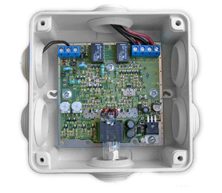
In precision electronics manufacturing, maintaining optimal environmental conditions is critical for product quality and equipment longevity. By integrating Filter Monitoring system, manufacturers can achieve predictive maintenance of ventilation systems through real-time data collection and intelligent analysis. The system employs wireless sensors to track filter pressure differentials, temperature, and humidity, transmitting data via the LoRa network to a cloud platform for automated alerts and maintenance scheduling.
Key Application Scenarios
- Energy Efficiency Optimization
- Dynamic filter replacement cycles reduce fan energy consumption by over 15%.
- Real-time alerts prevent equipment overheating due to filter blockages.
- Example notification: “Eastern zone filter pressure threshold exceeded. Recommend replacement within 3 days.”
- Cost Reduction
- Eliminates manual inspections, cutting labor costs by up to 70%.
- Precise monitoring avoids premature filter changes, reducing annual spare part costs by ~30%.
- Risk Mitigation
- Instant leakage or clog detection triggers multi-level alerts (SMS/email/phone).
- Potential production disruptions are addressed within 24 hours.
- Data-Driven Insights
- Predictive algorithms forecast filter lifespan and seasonal contamination trends.
- Customizable dashboards support compliance with ISO 50001 energy standards.
Printed Circuit Board Examples
- Special Processes: Blind/Buried Vias, Impedance Control (±10%), Signal Loss <0.2dB/inch
- Standard Materials: FR4, HDI, High-Frequency Boards, High-Speed Boards
- Specialized Circuits: Flexible Circuits, Rigid-Flex PCBs, Metal Core PCBs, Ceramic PCBs
- Layer Capability: Up to 32 layers (any-layer HDI)
- Minimum Trace/Space: 0.05mm/0.05mm
- Surface Finishes: ENIG, HASL, OSP, Immersion Silver/Tin
- Copper Thickness: 1/3oz~12oz
- Compliance Standards: IPC-A-600G, IPC-6012 Class 2/3
Extended Applications
Apart from the above IoT monitoring system application case, we have supported different cases for different customers, including:
- Robotics: Motor temperature monitoring and preventive maintenance
- Security Systems: Intrusion detection in server rooms
- Motorcycle Electronics: Battery thermal management
- Solar Power Stations: Inverter performance tracking
- Medical Devices: Cleanroom pressure differential alerts
- Smart Home: Air purifier filter life notifications
- Stage Lighting: HVAC control for temperature-sensitive equipment
- Student Projects: Prototype environmental monitoring solutions
- Component Distributors: Warehouse condition monitoring
- LED Lighting: Heat dissipation management for high-power fixtures
For scenario-specific customization or demo data, please provide detailed requirements for further optimization.
Overall, the printed circuit board production process is a sophisticated dance of engineering and technology. It is the critical path that turns a design into a reality. Understanding this process helps in selecting the right manufacturing partner. This article has outlined the key stages, from material choice to final testing.
EBest Circuit (Best Technology) stands ready to be that partner for you. We combine advanced technology with deep expertise to deliver PCBs you can depend on. Our focus on quality, transparency, and partnership ensures your projects are in the best possible hands. Pls feel free to contact our team at sales@bestpcbs.com for a prompt and professional response.
FAQs
Q1: Why are tooling rails (process edges) necessary on PCBs?
- Tooling rails are blank strips added along the edges of a PCB panel to provide space for automated SMT equipment to grip and transport the board during assembly. They also accommodate fiducial markers and tooling holes essential for accurate component placement. The standard width ranges from 5mm to 8mm.
Q2: Do you provide detailed production progress tracking?
- Yes. We maintain a real-time Work-in-Progress (WIP) system that tracks each board’s status daily. Clients receive updates at key stages—from material preparation to final inspection—ensuring full transparency throughout production.
Q3: Which file formats do you accept for manufacturing?
- We support standard design formats including Gerber files (RS-274X), CAD data, and IPC-2581. For assembly, we require a Bill of Materials (BOM) and centroid (pick-and-place) files.
Q4: What is solder mask, and what is its function?
- Solder mask is a protective polymer layer applied over copper traces to prevent oxidation, avoid solder bridges, and insulate circuits. It ensures solder adheres only to exposed pads (e.g., component leads and vias), improving reliability.
Q5: What solder mask colors are available?
- We offer green, blue, black, red, white, yellow, and purple. Green is standard; other colors may involve longer lead times.
Q6: How long does SMT assembly take?
- If components are in stock, SMT requires 2–3 days, followed by 1–2 days for testing. Most orders can be shipped within one week after production begins. Complex designs or special materials may extend the timeline.
For further details or project-specific queries, contact us at sales@bestpcbs.com.