When a quiet FPGA output glitches as neighboring outputs switch, repeat the capture with a shorter probe loop and change the number of switching outputs before changing the board. Then compare three voltages: quiet pin to local ground, local ground to receiver ground, and supply to its own local ground. These readings answer different questions.
Consider a hypothetical 3.3 V FPGA interface where an otherwise low status line appears to cross the receiver’s low-level limit when eight outputs switch. The oscilloscope trace alone cannot tell whether the receiver sees ground motion, a rail dip, ringing on one net or a probe artifact. Here is how to separate those causes and prove the fix.
what is ground bounce
Ground bounce is a transient change in voltage between two points treated as ground. When several outputs switch, their current may share part of the package and board return path. The voltage across that path can move even though both ends are on the same schematic net. A receiver responds to the signal relative to its own reference, not the zero line printed on an oscilloscope.
For the FPGA example, define driver-side board ground and receiver-side board ground before measuring. The die ground inside the package usually is not accessible. A board-level capture cannot measure it directly. A quiet output can serve as an indicator of switching noise, but it is not a direct reading of the internal ground node.
what causes ground bounce
A first-order inductive estimate is V = L × di/dt. If, hypothetically, 0.75 nH of effective common inductance carries a 0.16 A change in 0.8 ns, the estimate is 0.15 V. At the same current change over 1.6 ns, it is 0.075 V. These are sensitivity estimates, not measured peaks; actual current waveform, distribution, package and interconnect response matter.
The example explains why a lower repetition rate may not fix the glitch. Switching less often does not necessarily slow each edge. Change the number of outputs, programmed slew or load in controlled steps and measure what actually changed. The TI simultaneous-switching application report explains quiet-output test methods and why package and test conditions matter.
simultaneous switching noise
Keep the observed status pin low and use a repeatable trigger. Run the same pattern with one, four and eight outputs changing together; record direction, slew, drive strength, load, I/O bank, test points and terminations. Use the actual receiver or a known equivalent load. Compare both switching directions and capture multiple repetitions, not just a favorable screenshot.
| Parameter | Hypothetical comparison | Control |
| I/O rail | 3.3 V nominal | Same receiver and rail setting |
| Aggressor count | 1, 4 and 8 | Same bank, load and switching edge |
| Quiet status pin | Held low | Same pin, node pair and trigger |
| Programmed slew | Default then one approved slower setting | Keep other settings fixed |
| Release limit | Receiver input and system timing limits | Evaluate measured waveform and functional errors |
oscilloscope probe ground spring
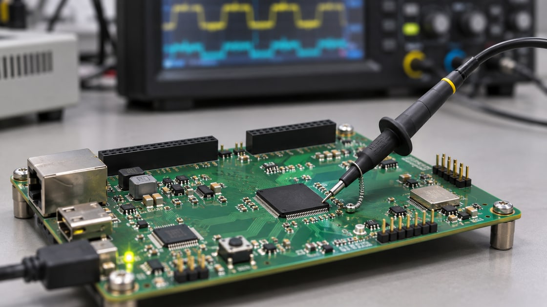
A long ground clip can add loop inductance and pick up a nearby edge. Compare it with a ground spring on a suitable local return point, using the same probe, scope bandwidth and signal node where practical. A repeatable change with the probe arrangement is evidence of measurement sensitivity, not proof that the board has no problem. Document the geometry for any comparison.
Standard bench-scope ground clips are usually connected to protective earth and to one another. Do not clip them to nodes that must remain isolated, and do not defeat protective earth. For a ground-to-ground difference or a small differential voltage on a noisy common-mode level, use a suitable rated differential arrangement within its voltage, bandwidth and common-mode limits.
ground bounce measurements
Start with the status pin against the local return. Then use a differential measurement for the two ground points where practical, and measure the rail directly across nearby power and ground pads. If the issue is receiver behavior, also capture the signal at the receiver relative to receiver ground. Use comparable loading and bandwidth, then correlate the captures against the same switching event.
| Node pair | What it measures | What it cannot establish alone |
| Status pin to driver-side ground | Quiet output deviation near the driver | Actual input waveform at the receiver |
| Driver ground to receiver ground | Local board-reference movement | Internal package ground motion |
| I/O supply to its local ground | Local supply excursion | Noise between two board ground points |
| Receiver pin to receiver ground | Actual receiver input margin | Which source created the excursion |
simultaneous switching noise analysis
If the anomaly shrinks mainly when the probe loop changes, fix the setup and retest. If reference movement grows with output count and the receiver trace moves with it, investigate shared return and package/I/O choices. If the rail falls relative to its own return and the timing follows the rail disturbance, investigate the power delivery path. If one net rings while other measurements stay quiet, evaluate that net’s termination and discontinuities.
These are competing hypotheses, not mutually exclusive labels. Compare a known-good capture and change one variable at a time. Use the PCB power integrity guide when rail measurements point to a supply problem rather than a moving signal reference.
decoupling capacitor placement
Move or revise decoupling when the power-to-local-ground capture supports a supply-loop issue. A long neck or remote via pair can make a nearby-looking capacitor electrically far away at fast edges. Check the loop through package power, board vias, capacitor and reference return. Adding more capacitance does not bypass a broken return path and can change the PDN response.
If the rail is in budget and the receiver reference moves, compare a slower supported output setting or bank redistribution before changing the capacitor count. The trade-off is timing or pin-planning effort. A layout change to repair a shared return costs a new build but may be needed if configuration changes do not provide enough margin.
pcb ground plane rules
Trace the return path near the offending I/O bank and at every layer transition. Check the reference plane for voids or splits, nearby return vias, connectors and narrow ground necks. A layout correction cannot remove every package-internal effect; follow the device documentation for bank assignments and permitted switching conditions. See the via stitching guide for board return transitions.
Release the fix only when the worst approved switching pattern stays inside the receiver’s guaranteed input and timing limits with the agreed margin across required corners and no functional errors in the agreed test. Save the setup photo, revision, test nodes, I/O configuration, waveform and error counts. A cleaner screenshot at one temperature is not a release criterion.
FAQ
Can a long scope ground lead create a false ground-bounce trace?
Yes. A long loop can pick up nearby fields and produce ringing with the probe input. Recheck at the same signal point using a short local reference and a suitable probe. If the shape changes materially, record that effect before interpreting amplitude or using the original capture to justify a layout change.
Is ground bounce the same as supply droop?
No. Ground bounce compares reference points; supply droop is a drop in a rail relative to its own local ground. Both can occur during the same switching event. Measure both quantities separately and then confirm the voltage actually presented to the receiver rather than trying to infer it from a remote rail test point.
Why does the low output move if it never toggles?
A quiet low output can show switching noise because its output structure references a return path used by active outputs. That response may also include coupling or measurement artifacts. Keep the quiet output loaded as intended and compare how the disturbance changes with switching count, direction, probe setup and chosen reference.
Does slowing the clock eliminate ground bounce?
Not necessarily. A lower clock can reduce how often the event occurs, but each edge may still be fast and the same outputs may switch together. If the device permits it, compare output slew or switching alignment while checking timing. Keep the receiver load and trigger fixed for a meaningful comparison.
Should I add a larger decoupling capacitor first?
Not without rail evidence. A larger capacitor may help a slower supply excursion yet do little for a high-inductance local loop or a shared ground path. Measure across local power and ground, then evaluate placement, via geometry and impedance. Verify that a changed capacitor does not create another problem in the measured band.
Is ground bounce always worse on a two-layer PCB?
No. Package behavior, edge rate, load, stackup, routing and return geometry all matter. A second layer with a continuous usable reference can be better than several badly interrupted planes. Inspect the actual signal and return paths and confirm with a controlled measurement; layer count alone cannot qualify the interface.
Can I use two passive probes to measure between grounds?
Only with a safe setup and understood bandwidth, probe matching and common-mode error. Ordinary bench-scope ground clips are generally connected together through earth, so placing them on different nodes can disturb or short the circuit. Prefer a suitable rated differential method when that connection or accuracy is a concern.
What waveform proves the fix worked?
Measure the receiver pin against its own reference during the agreed worst-case switching pattern. Use device-specific guaranteed input levels and timing requirements, including the project’s required margin. Repeat at the necessary operating conditions and record functional errors, not just peak voltage; keep the probe setup fixed between baseline and revised captures.
Technical References
- TI: Simultaneous-Switching Performance of TI Logic Devices
- TI: Design Considerations for Logic Products
Request a Fabrication Review
For a Best Technology PCB stackup or layout review, send the board revision, return-path layout, I/O bank and switching pattern, probe reference points, and a failing and known-good capture. Include the receiver limits and the exact verification condition.
You may also like
Tags: FPGA PCB, PCB Ground Bounce, Signal Integrity, Simultaneous Switching Noise