





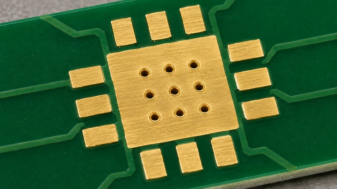
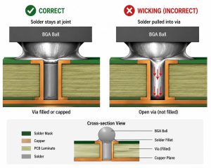
Thermal via solder wicking happens when molten solder enters a via opening connected to a package’s exposed land. On a power QFN, that can reduce solder remaining under the package or leave solder on the opposite side. Prevent it by deciding together which vias remain open, where paste is printed and what the assembly inspection must confirm.
Do not remove thermal vias just to make the solder process easier. Compare the via treatment and stencil pattern against the package guidance, electrical connection, thermal target and fabrication capability, then verify the assembled joint on representative hardware.
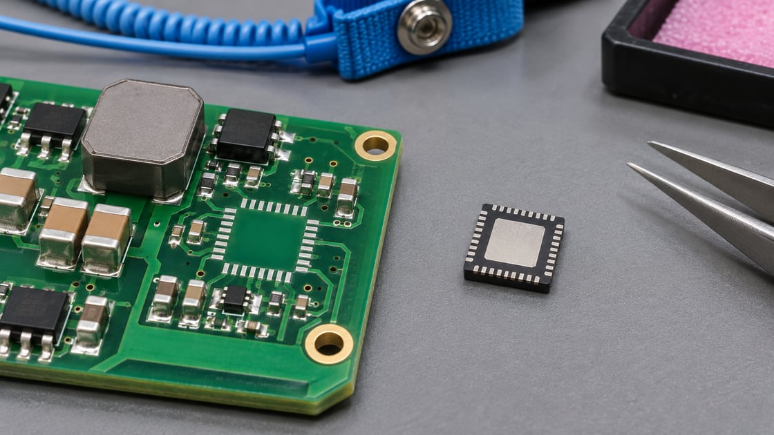
thermal via solder wicking
An open, wettable via inside the pasted land creates a path for solder during reflow. The amount that enters depends on the opening, plating and wetting, available solder and process conditions. It is not enough to count vias or compute their empty volume. TI’s PowerPAD application report discusses controlling hole size and stencil placement for the packages it covers.
Check the actual joint for loss of solder and the reverse side for protrusion or deposits. Do not label every exposed-pad void as wicking; outgassing and paste or reflow behavior can also contribute.
thermal pad via design
Design the thermal and assembly paths as one set of requirements. The exposed pad may have an electrical connection as well as a thermal role; check its required net in the device datasheet. Draw the via array, finished hole openings, paste windows and mask openings on the same coordinate basis so both suppliers can review them.
| Parameter | Specify or verify |
| Finished hole | Diameter and location |
| Via treatment | Open, tented or capped |
| Paste windows | Size and alignment |
| Thermal path | Net, planes and copper |
| Evidence | X-ray and thermal check |
thermal vias size and spacing
Use the exact package recommendation and fabricator capability, not a universal hole diameter or pitch. Smaller openings may limit the solder available to flow into a barrel, but hole size, plating and pitch also affect the heat path and manufacturing yield. In a solder-risk review, ask where each opening lands relative to the stencil windows and what registration margin remains.
The thermal via design overview covers the separate heat-flow and resistance question. This article focuses on deciding which openings can safely remain beneath the soldered land.
should thermal vias be tented
Tenting is an option only if the selected side and mask process are suitable for the package and assembly route. A mask film spanning an opening is not a metal cap. Top-side tenting can affect the wettable pad area; reverse-side tenting leaves a top-side opening unless the stack or process specifies otherwise.
Ask whether the supplier can maintain the requested tent through fabrication and reflow at the finished hole size. Compare this with paste windows that avoid open vias, rather than treating tenting as a universal remedy.
thermal via filling
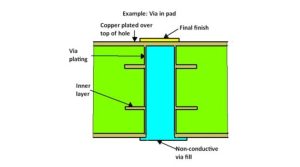
Specify what “filled” means before comparing quotes. A resin-filled via with a metal cap presents a different top surface from an open plated hole; a tented or merely plugged hole is not automatically planar or capped. A nonconductive fill does not remove the existing plated copper path, but it should not be modeled as a solid copper cylinder.
| Option | Top surface | Check before release |
| Open plated via | Opening exposed | Paste clearance |
| Mask tent | Mask film, if intact | Side and coverage |
| Filled and capped | Plated surface | Flatness and cap integrity |
via in pad plated over
Filled and plated-over via-in-pad can be useful when an uninterrupted solderable land is needed. Confirm the fill, cap plating, finished planarity and inspection evidence rather than approving a quote based only on “VIPPO.” See the via-in-pad plated-over process guide for manufacturing details.
Compare the extra process requirements with an open-hole approach that positions stencil windows away from the vias. Both options need assembly verification. Capping addresses the open-hole path but does not remove every possible cause of voiding.
qfn ground pad stencil design
Segmenting the paste area can help the assembler control deposit distribution and avoid some open holes. Use the package and assembly process recommendations; the stencil thickness and pattern must also suit the peripheral joints. TI’s QFN and SON attachment guidance discusses exposed-pad stencil options and X-ray evaluation.
For a drawing check only, four 1.2 mm square windows on a 3.0 mm square exposed land occupy 5.76 mm² of the 9.00 mm² land, or 64% area. With a 0.10 mm stencil, their theoretical aperture volume is 0.576 mm³. Neither value is a recommended target or a prediction of deposited solder; transfer efficiency and reflow change the result. Inspect the actual printed pattern before treating the layout as qualified.
qfn solder void
Look at the void pattern, remaining joint coverage and any solder on the reverse side together. A two-dimensional X-ray can help locate voids, but it does not by itself prove how a void formed or how much solder entered a specific via. Compare the image with the via locations, stencil layout and process records.
Before approving the design, agree the package-specific acceptance criteria with the assembly team. If the cause is still unclear, choose targeted cross-sections or another agreed inspection. Check the assembled board’s temperature under representative power and ambient conditions; a neat-looking X-ray is not a thermal qualification.
FAQ
Does every open thermal via wick solder?
No. The via and land must interact with molten solder under the actual process conditions. The risk depends on wetting, hole geometry, paste placement and reflow. Inspect both sides of representative assemblies and check the joint before treating a given arrangement as safe.
Is tenting on the bottom the same as a filled and capped via?
No. A mask tent can cover one opening but does not create a plated, planar top land. A filled and capped via uses a different fabrication sequence. Ask for the treatment and inspection details in the fabrication drawing instead of relying on an abbreviated label.
Can I simply reduce the amount of paste to stop wicking?
Reducing paste everywhere can leave an insufficient joint even if less solder travels down the hole. First review where paste overlaps the openings and what the package guidance calls for. Use measured paste deposits and assembled-joint evidence rather than adjusting total paste area alone.
Why are there solder deposits on the opposite side of the board?
An open via connected to the land can be a route for solder during reflow, but other solder processes can also leave deposits. Correlate their locations with the via map and record the assembly sequence. Inspect the top joint rather than assuming the reverse deposit is harmless.
Can a large void prove the exposed pad is not soldered?
A single X-ray view can show a projected void, not the full thickness or shape of a joint. Compare the image with the agreed criteria and inspect the location relative to the pad and vias. Use a suitable follow-up method if the diagnosis affects acceptance.
Will resin-filled vias provide the same thermal result as copper-filled vias?
Do not assume that they will. The barrel, fill, cap and connected planes contribute differently to heat flow. Use the actual cross-section and material properties in a thermal model, then confirm the assembled board when the temperature margin is small.
What must I tell the fabricator before selecting a via treatment?
Provide the package drawing, exposed land and via locations, finished hole sizes, affected sides and required surface condition. Also identify which features must be inspected and whether the assembler expects a flat solderable land. Get the treatment description accepted before releasing the files.
Should I compare a modified stencil using the same assembly process?
Yes, when practical. Keep the package, board, paste and reflow conditions comparable so changes are attributable to the stencil trial. Record print results, joint images and thermal checks together. If several inputs change at once, do not attribute the result to one adjustment alone.
Discuss Your Project
Send Best Technology the device drawing, pad and via layout, finished hole sizes and preferred treatment. Include the stencil and inspection requirements if they are already agreed. Contact sales@bestpcbs.com.
You may also like





Tags: QFN Assembly, solder wicking, thermal vias, via in pad
