





Why does an energy system monitoring PCB board perform accurately in the laboratory but show current measurement errors, unstable ADC readings, or localized overheating after installation in an inverter or industrial power system? Why can production batches behave differently even after the prototype passes testing? The causes may be related to sensing connections, PCB layout, insulation structures, or assembly quality.
An energy system monitoring PCB board must meet requirements for measurement accuracy, EMI performance, electrical safety, and production consistency. EBest Circuit provides custom PCB fabrication, component sourcing, SMT/THT assembly, and functional testing services for industrial energy monitoring equipment, from prototypes to mass production.

What Types of Energy System Monitoring PCB Boards Are Used in Industrial Power Systems?
An energy system monitoring PCB board can be used in several types of electrical monitoring equipment, each with different sensing and manufacturing requirements.
- Industrial Power Distribution Monitoring PCBs: Measure AC voltage, current, active power, power factor, and operating conditions. These boards commonly integrate voltage sensing, current sensor interfaces, metering ICs, and communication circuits.
- Battery Energy Storage Monitoring PCBs: Collect battery voltage, charge/discharge current, temperature, and operating data. Stable DC sensing and reliable electrical connections are critical.
- Solar Inverter Monitoring PCBs: Monitor DC bus voltage, AC output, and fault conditions while operating near high-frequency switching circuits.
- Industrial Energy Data Acquisition PCBs: Integrate multiple sensing channels, microcontrollers, data logging, and interfaces such as RS-485 or CAN.
An energy monitoring PCB does not necessarily carry the main power current. For example, if a 50 A battery current passes through an external busbar and shunt resistor, the monitoring PCB receives only the sensing voltage.
The monitoring PCB does not need copper conductors sized for the full 50 A unless that current actually passes through the board.
What Electrical Specifications Must Engineers Confirm Before PCB Manufacturing?
Working voltage, measurement range, accuracy, PCB construction, copper weight, operating temperature, and insulation requirements should be defined with measurable values.
The following examples describe potential engineering specifications for a 48 V battery energy monitoring board and a separate 400 V DC bus monitoring board.
| Parameter | Engineering Example | Manufacturing and Verification Requirements |
|---|---|---|
| Working voltage | 48 V nominal, 40–60 V DC measurement range; separate 0–450 V DC application | Maximum continuous voltage, transients, component ratings |
| Current range | 0–50 A DC, 50 A continuous | Onboard or external shunt, actual current path |
| Current sensing | 1 mΩ shunt, 50 mV at 50 A | Kelvin connections, amplifier input range, temperature drift |
| Measurement accuracy | Example target: ±0.5% of reading from 5–50 A | Calibration conditions, zero-offset limits, acceptance criteria |
| PCB construction | 4-layer FR-4, 1.6 mm board thickness | Stackup, reference planes, impedance requirements, tolerances |
| Copper weight | 1 oz, approximately 35 μm nominal copper foil, for a signal-processing PCB | Actual current path, conductor temperature rise |
| Trace and hole dimensions | Low-voltage signal area: 0.15/0.15 mm trace/space, 0.30 mm finished hole | Fabrication capability, pad geometry, hole plating |
| Operating temperature | Example: −20°C to +70°C | Component temperature ratings, derating, thermal performance |
| Electrical isolation | Basic or reinforced insulation as required by the equipment | Creepage, clearance, material group, isolation slots |
| Communication | RS-485 or CAN | Transceiver ratings, termination, communication testing |
These values are illustrative design inputs, not universal PCB requirements or guaranteed EBest Circuit manufacturing capabilities.
A 2-layer FR-4 PCB may be sufficient for a simple low-speed monitoring circuit. A 4-layer board generally provides more flexibility when analog sensing, digital control, and communication interfaces need separate routing and continuous reference planes.
A 0.15 mm spacing suitable for ordinary low-voltage signal traces must not be automatically applied to a 400 V isolation boundary. High-voltage spacing must be established separately using the applicable insulation requirements.
Why Do Energy Monitoring PCBs Experience Voltage and Current Measurement Errors?
Current sensing errors should be investigated at the shunt resistor and Kelvin connections. Voltage measurement errors require checking the divider ratio, component voltage ratings, and ADC input conditions.
Consider a 1 mΩ current-sensing resistor carrying 50 A:
- Expected shunt voltage: 50 A × 1 mΩ = 50 mV
- Additional 0.05 mΩ resistance included in the sensing path produces 2.5 mV of unwanted voltage drop.
- If the additional drop is included in the measured voltage, the resulting gain error is approximately 5%.
The sensing traces should connect to the specified shunt sensing points rather than arbitrary locations on high-current copper conductors. Four-terminal shunts should use their dedicated Kelvin connections as specified by the component manufacturer.
For voltage measurement, consider a 400 V DC bus connected to a divider with a 1.99 MΩ upper resistance and 10 kΩ lower resistance.
The ideal output is:
400 V × 10 kΩ ÷ (1.99 MΩ + 10 kΩ) = 2.00 V
However, the correct nominal output voltage does not establish that the circuit is safe or sufficiently accurate.
At 400 V, the total upper divider resistance dissipates approximately 0.080 W. Engineers must also check resistor voltage ratings, individual resistor power dissipation, series resistor distribution, and ADC acquisition time.
Measurement symptoms help narrow the problem:
- Error increases proportionally with the input: Check shunt resistance, divider ratio, and sensing gain.
- Error is greatest at low current: Check amplifier offset, ADC zero offset, and low-level noise.
- Readings drift with temperature: Check resistor temperature coefficients and voltage reference stability.
- Errors vary between batches: Check component tolerances, part numbers, and calibration data.
The final accuracy must be evaluated against the complete circuit error budget and verified through measurement testing.
How Can PCB Layout Reduce Noise and EMI in Energy Monitoring Circuits?
Start with the physical relationship between sensing traces and switching nodes. Then check return-current paths and input filtering.
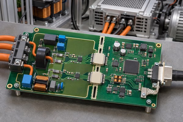
- Sensing traces: Keep millivolt-level signals away from MOSFET switching nodes, power inductors, and high-di/dt loops. Route differential inputs according to the measurement IC manufacturer’s layout guidance.
- Reference planes: Maintain suitable return paths and avoid unnecessary ground-plane splits beneath sensitive traces.
- Decoupling: Place the specified supply bypass capacitors near the relevant IC supply pins to minimize high-frequency current-loop area.
- Input filters: Select RC filters according to noise rejection and required measurement bandwidth. Mismatched components on differential inputs can reduce common-mode noise rejection.
How can engineers determine whether EMI is responsible?
Compare ADC readings with switching disabled, normal PWM operation, and high-load operation.
If noise appears only while switching is active, examine coupling from switching nodes, supply ripple, and ground return paths.
If the error remains approximately proportional to the input under all operating conditions, check gain, resistor values, and calibration before changing the PCB construction.
What Are the Isolation and Safety Requirements for High-Voltage Energy Monitoring PCBs?
Determine the required insulation type before calculating clearance and creepage distances. A 400 V operating voltage alone does not justify a universal 3 mm, 6 mm, or other fixed spacing.
For a DC bus monitoring PCB, inspect:
- High-voltage boundaries: Identify the insulation required between hazardous sensing circuits, microcontrollers, and accessible communication interfaces.
- Conductors and pads: Check actual spacing between copper features, vias, connector terminals, and component leads.
- Mounting structures: Assess whether screws, metal fixtures, or nearby conductive structures affect insulation paths.
- Isolation slots: Confirm slot dimensions, positions, and fabrication tolerances and their actual effect on creepage.
- Materials and components: Verify the laminate CTI group, isolation component ratings, and connector insulation properties.
IEC 60664-1 provides insulation coordination requirements within its applicable scope. The calculation also depends on working voltage, transient overvoltage, pollution degree, overvoltage category, insulation type, material group, and operating altitude.
For example, two systems operating at the same 400 V DC level may require different insulation arrangements if one operates inside a controlled enclosure while the other is exposed to condensation or contamination.
PCB manufacturing must reproduce the approved spacing, slots, and materials. Final product safety compliance requires the applicable equipment-level verification.
How Can PCB Copper Layout and Component Placement Prevent Overheating?
Shorten high-current paths, eliminate narrow copper bottlenecks, provide suitable heat-spreading copper, and separate precision sensing components from major heat sources.
How should copper be routed?
- Use wider, shorter current paths: At the same copper thickness and current, longer or narrower conductors generally have higher resistance and I²R losses. Avoid unnecessary high-current routing loops.
- Remove narrow neck-downs: A 10 mm-wide copper path that suddenly narrows to 1 mm near a connector or pad can create a localized hot spot. Check the entire current path rather than only its widest section.
- Use suitable copper pours: Provide continuous copper connected to the appropriate electrical net to spread heat, while maintaining all required insulation distances.
- Add thermal vias where useful: For regulators and power devices with thermal pads, connect the appropriate copper layers through thermal vias according to the component’s layout recommendations. Control solder wicking and assembly requirements.
- Preserve isolation boundaries: Thermal copper and vias must not bridge hazardous-voltage and accessible low-voltage regions.
How much can wider copper reduce power loss?
Consider a 50 mm-long copper conductor with 1 oz nominal copper thickness, approximately 35 μm. Using copper resistivity near 20°C:
- 10 mm width: Resistance approximately 2.46 mΩ; at 10 A, power loss approximately 0.246 W.
- 20 mm width: Resistance approximately 1.23 mΩ; at the same 10 A, power loss approximately 0.123 W.
With otherwise identical conditions, doubling trace width approximately halves conductor resistance and I²R power loss.
These are simplified resistance calculations, not validated current-carrying ratings. Actual allowable current depends on temperature rise, PCB construction, copper layers, mounting, and thermal conditions.
Where should the components be placed?
- Shunt resistor: Place it near a suitable high-current connection area to minimize unnecessary current-path length. Route dedicated Kelvin sensing connections from the specified terminals.
- High-current connectors: Avoid forcing current through repeated narrow copper sections or unnecessary layer transitions. Verify connector current ratings and soldering arrangements.
- Power regulators: Provide copper area and thermal vias where required by the component’s thermal-pad layout.
- ADCs, precision references, and sensing amplifiers: Keep them away from concentrated heat sources such as shunts, power inductors, and regulators to reduce temperature gradients and measurement drift.
Finally, verify temperatures at the maximum specified ambient temperature, continuous operating load, and actual installation conditions.
Measure the shunt, connectors, power regulators, and nearby PCB areas. Acceptance must be based on component temperature limits, derating curves, and system thermal requirements.
IPC-2152 provides guidance for evaluating conductor sizing and temperature rise. A single generic current-versus-trace-width number is not sufficient for production approval.
What Causes Energy Monitoring PCB Failures When Moving From Prototype to Mass Production?
Check critical BOM changes, soldering consistency, document revisions, and calibration data first.
- Precision component substitutions: Replacing a 0.1% shunt resistor with a 1% version may invalidate the measurement error budget. Temperature coefficient, power rating, and package details also require review.
- Critical solder joint defects: Poor shunt or connector joints can introduce additional resistance, localized heating, or intermittent operation.
- Revision mismatches: Using updated Gerber files with outdated BOMs, placement data, or assembly drawings can create component and footprint errors.
- Firmware or calibration differences: Changes in zero-offset, gain coefficients, or firmware revisions may affect measurement consistency between batches.
Before mass production, use a single approved set of Gerber files, BOM, assembly drawings, placement data, firmware, and test requirements.
First-article inspection should confirm component identification, placement, and soldering. Pilot production should verify actual sensing channels and product functionality.
Successful power-up alone is not sufficient evidence of production consistency.
How Are Energy System Monitoring PCB Assemblies Inspected and Functionally Tested?
Testing should cover electrical connections, assembly quality, power operation, measurement accuracy, and communication, with explicit acceptance criteria for each stage.
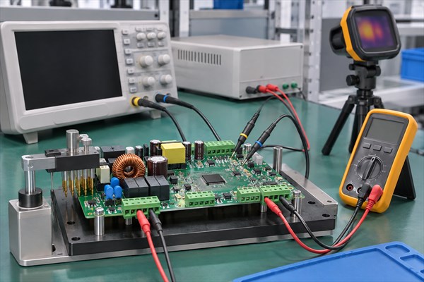
| Test | What to Check | Acceptance Basis |
|---|---|---|
| Bare-board electrical testing | Opens, shorts, net connectivity | Approved PCB netlist |
| Assembly inspection | Part numbers, orientation, solder quality | BOM, assembly drawings, applicable workmanship criteria |
| Power-up testing | Supply rails, startup current, reset behavior | Customer-defined electrical limits |
| Measurement testing | Offset, gain, measurement range, error | Approved test points and accuracy limits |
| Communication testing | Data transmission, configuration, protocol responses | Interface and protocol test procedures |
| Special verification | Insulation, dielectric, environmental tests | Applicable requirements and approved test procedures |
For a 50 A full-scale current monitoring board, an agreed test plan might include 0 A, 5 A, 25 A, and 50 A.
If the required accuracy is ±0.5% of reading from 5 A to 50 A:
- At 5 A: ±0.025 A
- At 25 A: ±0.125 A
- At 50 A: ±0.25 A
A separate absolute offset limit is necessary at zero; a percentage-of-reading limit alone is not suitable.
The test specification must also define reference instruments, operating temperature, supply conditions, acquisition settings, and any unit-level calibration requirements.
High-voltage dielectric or insulation testing requires suitable fixtures and approved safety procedures.
EBest Circuit supports PCB electrical testing, assembly inspection, and customer-specified functional testing within the agreed project scope. Custom fixtures, calibration procedures, and special qualification tests should be confirmed before production.
What Factors Affect Energy System Monitoring PCB Manufacturing and Assembly Costs?
PCB layer count, copper weight, precision components, assembly processes, and test coverage are the primary cost drivers for a complete energy monitoring PCBA.
- PCB construction: If four layers already provide adequate routing and reference planes, increasing to six layers may not deliver a practical benefit.
- Copper weight: Heavy copper may be unnecessary when the main current flows through an external busbar instead of the monitoring PCB.
- Precision components: Shunts, metering ICs, isolation devices, and industrial connectors can significantly affect BOM cost.
- Assembly complexity: Double-sided SMT, fine-pitch packages, through-hole connectors, and special soldering add manufacturing operations.
- Testing requirements: Multi-channel measurement verification, firmware programming, calibration, and dedicated fixtures must be included in the production scope.
Cost optimization should first target unnecessary manufacturing requirements, not essential safety checks or measurement tests.
Supplier quotes should be compared using the same fabrication, BOM, substitution, assembly, and acceptance requirements.
Why Choose EBest Circuit for Energy System Monitoring PCB Manufacturing?
EBest Circuit provides PCB fabrication, component sourcing, SMT/THT assembly, and functional testing coordination, reducing the effort customers spend managing manufacturing documents, components, and delivery requirements across different suppliers.
- Free DFM check: Review copper spacing, finished holes, pads, isolation slots, and assembly manufacturability to identify issues before production.
- Custom PCB fabrication: Manufacture 2-layer and multilayer PCBs according to approved Gerber files, stackups, board thicknesses, copper weights, and surface finishes.
- Integrated PCB and PCBA services: Coordinate bare-board fabrication, component sourcing, SMT/THT assembly, and inspection under one project.
- Critical BOM verification: Check specified precision resistors, measurement ICs, isolation components, and connectors. Component substitutions follow customer approval requirements.
- Inspection and functional testing: Support agreed manufacturing checks and customer-defined functional verification.
- Prototype-to-production support: Manufacture prototypes, pilot batches, and repeat orders using approved documentation and assembly requirements.
Relevant quality management certificates, manufacturing capabilities, and inspection documentation can be reviewed during supplier qualification.
FAQs About Energy System Monitoring PCB Boards
Q1: Can one energy monitoring PCB measure both AC and DC power?
A1: Yes, provided its sensors, sensing circuits, and measurement ICs support the corresponding conditions. AC and DC measurement ranges and calibration should be verified separately.
Q2: Can an energy monitoring PCB measure bidirectional charge and discharge current?
A2: Yes. The sensing IC must support bidirectional measurements and correctly handle current polarity and zero-offset errors.
Q3: Does multiphase energy monitoring always require simultaneous-sampling ADCs?
A3: No. Accurate phase-angle and multiphase power calculations require careful timing control. Non-simultaneous sampling is suitable only when its timing errors meet the measurement requirements.
Q4: Can an energy monitoring PCB preserve measurements before a power outage?
A4: Yes, with nonvolatile memory, suitable firmware, and an appropriate power-loss handling strategy. Saving the final measurement also depends on available hold-up time.
Q5: Does every RS-485 monitoring node need a 120 Ω termination resistor?
A5: No. For a typical RS-485 bus with approximately 120 Ω characteristic impedance, termination is normally applied at the two physical ends of the bus. The actual configuration depends on cable characteristics and network topology.
Q6: Does an energy monitoring PCB always require conformal coating?
A6: No. Coating may be appropriate for humid, condensing, or contaminated environments. Material compatibility, masking, and insulation requirements must be verified.
Q7: Can firmware programming and calibration data loading be included in PCBA production?
A7: Yes, when firmware files, programming interfaces, calibration data, fixtures, and acceptance procedures are provided and included in the agreed production scope.
Q8: Can an energy monitoring PCB measure harmonics and power factor?
A8: Yes, with suitable sensing hardware, bandwidth, channel synchronization, and processing algorithms. Basic voltage and current monitoring does not automatically provide full power-quality analysis.
How Can You Request a Custom Energy System Monitoring PCB Quote?
Are measurement errors, EMI interference, high-voltage isolation issues, or inconsistent production results affecting your energy monitoring PCB project? EBest Circuit provides custom energy system monitoring PCB board manufacturing and PCBA assembly for industrial power distribution monitoring, energy storage systems, solar inverter monitoring, and energy data acquisition equipment. Services include prototypes, component sourcing, SMT/THT assembly, and functional testing support.
Would you like a free DFM check before prototype or mass production? Send your Gerber files, BOM, assembly drawings, technical specifications, order quantity, required delivery date, and delivery location to sales@bestpcbs.com. Include specific component lot or date code requirements where applicable. EBest Circuit can review PCB fabrication and assembly feasibility and provide a custom quotation with an appropriate lead time.
You may also like



Tags: Energy Monitoring PCB Assembly, Energy Monitoring PCB Manufacturing, Energy System Monitoring PCB Board, Industrial Power Monitoring PCB