

PCB fabrication Singapore stands for excellence in the electronics industry. This guide will show you why Singapore is a hub for quality and how to navigate it successfully.
You might be wondering, what are the real challenges when sourcing PCBs for a Singapore-based project?
- Slow turnaround times that push back your product testing and launch schedules.
- Inconsistent quality leading to board failures, reworks, and wasted resources.
- Limited customization options from suppliers who only offer standard, off-the-shelf solutions.
- Unclear and unpredictable pricing that makes project budgeting a difficult task.
- Poor communication and support from distant manufacturers, creating frustrating delays.
Fortunately, these common pain points have clear solutions. By choosing a manufacturer built for the Singapore market, you can overcome these obstacles effectively.
- Guaranteed fast-track production ensures your prototypes and batches arrive exactly when you need them.
- A rigorous quality management system at every production stage delivers boards you can trust.
- A strong focus on flexible engineering supports complex, custom designs from the ground up.
- Transparent and upfront costing provides clarity from the first quote, with no hidden fees.
- A dedicated, responsive support team acts as your single point of contact for smooth collaboration.
With 19 years of expertise since 2006, EBest Circuit (Best Technology) has established itself as Asia’s premier one-stop PCB and PCBA manufacturer, specializing in advanced substrates including metal core, ceramic and heavy copper boards up to 20 oz. Our complete turnkey solutions cover everything from design and component sourcing to assembly and box-build integration, backed by ISO9001 and IATF16949 certifications. Operating at a 260,000 sq ft monthly capacity, we combine engineering-grade support with rapid 24-hour prototyping to deliver reliable solutions from concept to mass production. For project consultation and instant quotes, contact our team at sales@bestpcbs.com.
Why Choose PCB Fabrication Singapore?
Singapore’s electronics market is demanding. It requires the highest standards. Why does PCB fabrication Singapore thrive?
- Demand for Quality: Local industries like aerospace and medical tech need perfect boards. There is no room for error.
- Need for Speed: The fast-paced market requires quick turnarounds. Rapid prototyping is essential.
- Customization is Key: Standard solutions often fail. Custom PCB Singapore services provide tailored fits for complex projects.
- Robust Supply Chain and Stability: Singapore boasts a resilient and well-integrated supply chain, minimizing disruptions. Its political and economic stability ensures reliable long-term partnerships and consistent material sourcing, which is crucial for continuous production.
- Access to Skilled Talent and Innovation: The country is a hotspot for engineering talent and R&D. Collaborating with local fabricators means tapping into a pool of experts who are adept at implementing the latest technologies and solving complex design challenges.
In summary, the Singapore market requires a supplier that can match its pace and precision.
PCB Manufacturer – EBest Circuit (Best Technology)
EBest Circuit (Best Technology) is a leading PCB manufacturer from China. We specialize in serving international clients, especially in Singapore. Our goal is simple: deliver high-quality boards quickly and without hassle.
Our core services include:
- Rapid Prototyping
- Expert PCB Design Support
- PCB Manufacturing and Assembly
- Small to Large Volume Production
For Singapore clients, we offer:
- Fast, clear communication.
- Quick sample shipping.
- Reliable after-sales support.
To sum up, we provide Singaporean customers with a reliable, responsive partner they can count on.
Why Choose EBest Circuit (Best Technology) – Our Advantages
What makes us the right choice for your PCB board fabrication Singapore needs? Here are our key advantages:
- Advanced Technical Skills: We handle complex orders with ease. This includes multi-layer boards, HDI, and rigid-flex PCBs.
- Total Production Flexibility: We support projects of any size. From a single prototype to full mass production.
- Transparent Pricing: We offer clear, upfront quotes. No hidden fabrication charges or surprises.
- Speed and Professionalism: We respect your time. Our efficient processes ensure on-time delivery and responsive support.
Ultimately, these advantages mean fewer delays, lower risk, and a smoother path from design to finished product for you.
Advanced PCB Fabrication Processes
We employ state-of-the-art manufacturing techniques and rigorous process control to meet the most demanding requirements of modern electronics. Our comprehensive capabilities, backed by detailed process specifications, ensure that your printed circuit boards are built to the highest standards of reliability, performance, and quality.
1. High-Layer-Count & Complex Multi-layer PCBs
Designed for complex, high-density interconnect designs requiring robust performance and stable signal integrity.
- Layer Capability: Standard production of 1 to 50 layers, with advanced engineering support for boards up to 100 layers.
- Board Thickness: Range from 0.4mm to 6.0mm (Standard), extending to a limit of 0.15mm to 10.0mm (Prototype).
- Material Expertise: We utilize a wide range of materials, including:
- FR-4 Series: Standard TG (130-140°C), Mid TG (150°C), and High TG (170-180°C) from suppliers like KB, ITEQ, and SY.
- High-Speed/Low-Loss Materials: For critical signal integrity (e.g., Low loss: M4, TU-872SLK; Middle loss: M6, TU-883; Ultra low loss: M7, TU-993).
- Controlled Impedance: Tight impedance tolerance control at ±5Ω (<50Ω) or ±10% (≥50Ω).
2. High-Density Interconnect (HDI) PCBs
Enabling miniaturization and higher performance with finer lines, smaller vias, and increased connection density.
- Microvia Technology: Laser-drilled microvias with diameters as small as 0.10mm (Standard) and 0.07mm (Limit), with a depth-to-diameter ratio of up to 1:1.
- Complex Build-up Structures: We specialize in various HDI structures, including 1+N+1, 2+N+2, 3+N+3, and Any-layer HDI using sequential lamination cycles.
- Fine Line Capability: Advanced Laser Direct Imaging (LDI) enables fine lines and spaces. For example, with 1oz base copper, we achieve 3.5/4.0 mil line/space (Standard) and 3.0/3.0 mil (Advanced) on outer layers.
3. Rigid-Flex PCBs
Combining the stability of rigid boards with the flexibility of dynamic circuits for durable, space-saving, and lightweight applications.
- Integrated Construction: Seamless integration of rigid and flexible layers, eliminating connectors and improving reliability.
- Material Selection: Use of polyimide-based flexible materials capable of withstanding repeated bending.
- Applications: Ideal for aerospace, medical devices, and wearable technology where space and weight are critical.
4. High-Frequency & High-Speed PCBs
Engineered for superior signal integrity in RF, microwave, and high-speed digital applications (e.g., 5G, Radar, ADAS).
- Specialized Materials: Expertise in processing PTFE (Rogers, Taconic series) and Ceramic-filled hydrocarbon materials (e.g., Rogers4350B, RO4003C) known for stable Dielectric Constant (Dk) and low Dissipation Factor (Df).
- Plasma Treatment: A critical process for ensuring reliable plating on challenging PTFE surfaces.
- Advanced Processes: Specific bake cycles and lamination structures (e.g., Core+Core) are employed to maintain material integrity and signal performance.
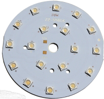
5. Metal Core PCBs (MCPCBs)
Designed for excellent thermal management in high-power LED lighting, power supplies, and automotive systems.
- Base Materials: Aluminum (1100/1050/5052, etc.) and Copper bases.
- Layer Count: 1 to 6 layers standard, with capabilities beyond 6 layers subject to engineering review.
- Thermal Conductivity: Support for dielectric layers with thermal conductivity ranging from 0.3 W/m.K to 12 W/m.K.
- Thermal Reliability: Capable of withstanding high operating temperatures and dissipating heat efficiently.
6. Comprehensive Surface Finish Options
A suite of finishes to meet specific application needs for solderability, durability, and performance.
- Lead-Free HASL: For general purpose applications (board thickness: 0.4-4.5mm).
- ENIG (Immersion Gold): Gold thickness: 0.025-0.125µm, Nickel thickness: 3-8µm. Ideal for fine-pitch components.
- ENEPIG (Electroless Nickel Electroless Palladium Immersion Gold): Excellent for wire bonding and preventing nickel corrosion.
- Immersion Silver/Tin & OSP: Cost-effective solutions for high-speed signals and short shelf-life requirements.
- Hard/Soft Gold Plating: For edge connectors (Gold Finger) and specialized applications.
7. Precision Mechanical & Electrical Performance
- Drilling Capabilities: Mechanical drill diameters from 0.15mm to 6.5mm, supporting aspect ratios up to 12:1 (Standard) and 25:1 (Limit).
- Copper Plating: Capable of producing extreme copper thicknesses up to 20oz (Inner) and 28oz (Outer) for high-current applications.
- Electrical Testing: 100% electrical testing with flying probe and test fixtures. Test parameters include max voltage of 5000V DC, max current of 200mA, and insulation resistance up to 100MΩ.
8. Rapid Prototyping & Accelerated Development Cycle
Our agile manufacturing flow and in-house engineering support ensure quick turnarounds without compromising quality, accelerating your product development from concept to reality.
- Quick-Turn Fabrication: Expedited processes for prototypes with stringent quality checks.
- Design for Manufacturing (DFM): Early engagement for design optimization to ensure manufacturability and cost-effectiveness.
In a nutshell, mastering this comprehensive suite of advanced processes allows us to consistently produce reliable, high-performance PCBs. From initial design support to final electrical testing, our integrated expertise ensures your boards meet the precise electrical, thermal, and mechanical requirements of your most challenging applications.
State-of-the-Art Equipment
Quality output is fundamentally rooted in top-tier manufacturing equipment. Our factories are equipped with the latest international machinery for imaging, plating, machining, and testing. This strategic investment translates into direct benefits for your products: superior precision, unwavering consistency, and exceptional competitive value.
1. Precision Imaging and Pattern Transfer Equipment
Our imaging processes ensure the accurate replication of circuit patterns, which is critical for high-density interconnect (HDI) and advanced designs.
- Laser Direct Imaging (LDI) Systems: Our advanced LDI equipment achieves fine line widths/spacing of 2.5/2.5 mil, meeting the stringent demands of high-frequency and high-speed boards.
- Automated Lamination and Exposure Lines: We use automated dry film lamination for consistent adhesion. Our exposure machines handle various dry film thicknesses (25μm to 50μm), ensuring precision for complex circuits.
2. High-Reliability Machining and Plating Equipment
The integrity of hole metallization is the core of multilayer PCB reliability. Our drilling and plating lines guarantee excellent precision and uniformity.
- CNC Drilling and Routing Machines: Our mechanical drilling equipment processes hole diameters from 0.15mm to 6.5mm, supporting an aspect ratio of up to 12:1 (e.g., a 0.2mm hole through a 2.4mm board). CNC routers perform precise outline machining.
- Advanced Electroless Copper and Electroplating Lines: We use leading-edge chemistry from suppliers like Rohm and Haas. Our process ensures a uniform electroless copper thickness of 1-3μm and precise copper plating for standard to heavy copper (up to 6oz) requirements.
3. Comprehensive Surface Finish and Automated Quality Assurance
We offer a wide range of surface finishes and employ rigorous testing protocols to ensure final product performance and quality.
- Automated Solder Mask and Legend Printing: Our automated solder mask coating and printing systems, including curtain coating, ensure perfect insulation. Legend printing achieves a minimum character width of 0.12mm.
- Precision Electrical Test and Measurement:
- Flying Probe Testers: Ideal for prototypes, testing up to 500V to ensure perfect circuit continuity and insulation.
- Advanced Analytical Instruments: Our lab is equipped with X-ray coating thickness gauges, ion contamination testers, and high-power microscopes (up to 1000x magnification) for cross-section analysis and meticulous quality control.
4. Automated Packaging and Shipping
- Vacuum Packing Machines: Every board is sealed using vacuum packing technology before shipment, protecting it from moisture and contamination to ensure it arrives in perfect condition.
How This Investment Benefits You:
- Higher Precision: From micron-level circuit traces to high-aspect-ratio vias, our equipment capabilities ensure your design is perfectly executed, resulting in better performance and reliability.
- Consistent Results: Highly automated processes and precise control guarantee that every production batch meets the same high standard, ensuring unwavering quality.
- Competitive Value: The advanced efficiency and high yield of our equipment allow us to optimize costs associated with PCB fabrication machine price, giving you superior quality without excessive cost.
To conclude, our continuous investment in state-of-the-art technology is a direct investment in the quality, reliability, and success of your products.
Rigorous Quality Control
At BES Technology, quality is not merely a final check but a core discipline integrated into every phase of our manufacturing process. Our systematic and data-driven approach ensures that every printed circuit board (PCB) we deliver meets the highest standards of performance and reliability.
Our Comprehensive QC Process Includes:
1. Incoming Material Inspection & Verification
We begin with a stringent verification of all raw materials, which are stored in a controlled constant temperature and constant humidity environment to preserve integrity. Key materials inspected include:
- Copper-Clad Laminates (Core): Thicknesses ranging from 0.05mm to 3.2mm.
- Copper Foil: Base copper weights from 1/3 oz (12μm) to 6 oz (210μm), with capabilities for special thick copper up to 20 oz.
- Prepreg (PP): Specific PP grades are selected to achieve precise dielectric thicknesses after lamination.
- Dry Film: High-precision films (25μm, 30μm, 40μm, 50μm) for accurate image transfer, stored in a yellow light safe zone.
2. In-Process Monitoring at Critical Stages
Real-time monitoring and verification are conducted at essential process points to prevent defects and ensure consistency.
- Inner Layer Fabrication: Post-etching, all inner layers undergo Automated Optical Inspection (AOI) to detect any line width anomalies or defects before lamination.
- Drilling Process: We enforce strict Aspect Ratios (board thickness to minimum PTH diameter) not exceeding 12:1 to ensure reliable plating. For a 0.2mm diameter hole, the maximum board thickness is 2.4mm.
- Plating Process: Panel Plating is monitored to uniformly build up copper thickness in holes and on surfaces, using advanced chemistry like HV-101 brightener for superior throwing power.
- Pattern Plating & Etching: Our process capability supports fine lines and spaces down to 2.5/2.5 mil. The tin plating acts as an etch resist to accurately define the final circuit pattern.
3. Final Comprehensive Testing and Verification
Before shipment, every board undergoes a final battery of tests to validate form, fit, and function.
- Electrical Testing:
- Flying Probe Test: Used for prototypes and small batches.
- Dedicated Test Fixture: Employed for volume production, with testing parameters up to 500V, 200mA, ensuring insulation resistance and continuity meet specifications.
- Final Quality Control (FQC): A comprehensive visual inspection is performed, aided by automated hole-counting equipment to verify completeness.
- Advanced Metrology: We utilize sophisticated tools for final validation:
- X-Ray Coating Thickness Gauge (CMI 900): For precise measurement of surface finishes like Ni/Au, Silver, and Tin.
- Impedance Tester: To verify controlled impedance on high-speed boards.
- Ionic Contamination Tester: Ensures boards are free from process-related residues that could impact long-term reliability.
This multi-layered, rigorous QC system, supported by advanced equipment and detailed process controls, is designed to proactively minimize risks. From material selection to final packaging, our unwavering focus is embedded in every step, guaranteeing that the PCBs you receive are not just compliant but truly dependable for your most critical applications.
Certifications and Industry Standards
Our commitments are verified by international standards. These certifications are proof of our reliability.
We hold:
- ISO 9001 (Quality Management)
- IATF 16949 (Automotive)
- ISO 13485 (Medical Devices)
- AS9100D (Aerospace)
All in all, these certifications give our Singaporean clients confidence that we meet the most rigorous international standards.
Case Study – Serving Singapore Clients
A Singapore-based client in medtech needed a complex HDI board. Their challenges were a tight deadline and a highly custom design.
Our solution:
- Provided PCB design Singapore support to optimize their layout.
- Delivered working prototypes in just one week.
- Seamlessly moved to batch production, meeting their launch date.
In closing, this partnership shows how we become a true extension of our client’s team to ensure success.
In conclusion, PCB fabrication Singapore demands a partner that matches its high standards. Quality, speed, and clear communication are non-negotiable.
EBest Circuit (Best Technology) is that partner. We bring advanced manufacturing, transparent practices, and a client-first approach to every project. For a quotation or to discuss your needs, contact us at sales@bestpcbs.com. We look forward to working with you.
FAQs
Q1: What is the flame retardant rating of your FR-4 PCB boards?
- A: Our standard FR-4 PCB boards consistently achieve a 94V-0 flame retardant rating under the UL94 standard. This indicates the material is highly self-extinguishing and meets stringent safety requirements for a wide range of electronic applications.
Q2: What is the maximum copper thickness you can manufacture?
- A: We specialize in heavy copper PCBs and can process copper thicknesses up to 30oz (1050μm). Our standard capabilities cover a wide range, from 1oz (35μm) to 6oz (210μm), with 70um(2oz) and 105um(3oz) being common for high-current applications. This is achieved through controlled processes like pattern plating, where we electroplate copper to build up the thickness on traces and in holes.
Q3: What is the minimum copper thickness you can produce?
- A: We can manufacture boards with a base copper foil as thin as 1/2oz (18μm). For even finer line designs, we also offer 12um (1/3oz) copper. These thinner coppers are essential for achieving high-precision, fine-line circuitry.
Q4: What does Tg (Glass Transition Temperature) mean in PCB laminates?
- A: Tg, or Glass Transition Temperature, is the critical point at which the solid base substrate (e.g., epoxy resin reinforced with glass fiber) begins to soften and transition into a rubbery state. A higher Tg value (e.g., Tg170, Tg180) indicates better thermal resistance, meaning the board can withstand higher operating and processing temperatures without deforming. This is a crucial factor for lead-free soldering processes and high-reliability applications. We use materials with appropriate Tg ratings to ensure dimensional stability during lamination, which is a high-temperature process, and long-term performance.
Q5: What is the maximum board size your X-ray equipment can scan?
- A: Our X-ray coating thickness gauge has a maximum loading capacity for boards up to 510mm x 420mm. The effective scanning area within this capacity is 435mm x 385mm. This equipment is vital for our quality control, allowing for non-destructive measurement of surface finishes like immersion gold (ENIG), silver, and tin, as well as internal features.
For further technical specifications or to discuss your specific project requirements, please contact our engineering team via sales@bestpcbs.com.