

An RF PCB manufacturer specializes in creating printed circuit boards for high-frequency applications. This is a field where precision is not just a goal; it is an absolute requirement. This article will guide you through the world of RF circuit boards, from fundamental concepts to advanced manufacturing capabilities.
Many engineers face significant hurdles when moving from standard PCBs to RF circuit PCB designs. What are the most common pain points?
- Signal Loss and Integrity Issues: The circuit looks perfect on screen, but the real-world performance is poor. Signals weaken or distort across the board, ruining data transmission.
- Impedance Mismatch: Achieving a consistent impedance is incredibly difficult. Even a tiny error in trace width or material thickness can cause signal reflections, degrading performance.
- Heat Management Problems: High-frequency operation generates heat. Standard PCB materials cannot dissipate this effectively, leading to overheating and potential failure.
- Manufacturing Inconsistency: A great design is useless if it cannot be built reliably. Many fabricators lack the tight process controls needed for RF work, leading to frustrating variations from board to board.
- Material Selection Confusion: The range of specialized RF laminates (like Rogers, Taconic, PTFE) is vast. Choosing the wrong material for your application’s frequency and thermal needs is a common and costly mistake.
Fortunately, these challenges have clear solutions. Partnering with a specialist RF PCB manufacturer transforms these obstacles into opportunities for optimal performance.
- Precision Engineering: They use advanced simulation software to model signal behavior before production. This ensures the final board maintains excellent signal integrity from input to output.
- Advanced Process Control: They maintain extremely tight tolerances on trace width, spacing, and dielectric thickness. This rigorous control is the only way to guarantee a perfect impedance match.
- Thermal Management Expertise: They understand the thermal properties of specialized materials. They select laminates that effectively dissipate heat and design stack-ups that manage thermal expansion.
- Certified Consistency: A top-tier manufacturer invests in state-of-the-art equipment and rigorous quality certifications like ISO 9001. Every batch meets the same high standard, every time.
- Material Guidance: They act as a consultant. Their engineers help you select the most cost-effective and performance-appropriate RF laminate for your specific project needs.
At EBest Circuit (Best Technology), we are a specialized RF PCB manufacturer focused on these exact solutions. Our team thrives on complex, high-frequency challenges. We combine deep material knowledge with cutting-edge fabrication processes to deliver boards that perform as promised. Feel free to contact us at sales@bestpcbs.com to discuss your project.
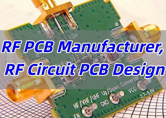
RF PCB Manufacturer – EBest Circuit (Best Technology)
EBest Circuit (Best Technology) is a leading RF PCB manufacturer with 19+ years of experience in high-frequency printed circuit board fabrication. We specialize in RF/microwave PCBs, high-speed digital PCBs, and hybrid RF-digital designs, offering full turnkey solutions from design to assembly.
Our expertise covers Rogers, Taconic, and other high-frequency laminates, ensuring optimal signal integrity for 5G base stations, radar, aerospace, and wireless communication applications.
1. RF PCB Materials & Stackups
We support a wide range of high-frequency materials with low dielectric loss (Df) and stable Dk:
- Rogers (RO4000®, RO3000®, RT/duroid®)
- Taconic (TLX, TLY, RF-35)
- Isola (IS680, IS410)
- PTFE-based laminates (for mmWave applications)
- Hybrid constructions (mixing FR4 with RF materials for cost optimization)
Typical Properties:
- Dk (Dielectric Constant): 2.2 – 10.2
- Df (Dissipation Factor): 0.001 – 0.004 @ 10GHz
- Copper Foil: Low-profile (≤1µm Ra) for reduced insertion loss
2. RF PCB Fabrication Capabilities
| Parameter | Standard Capability | Advanced Capability |
|---|---|---|
| Layers | 1-32L | Up to 50L (rigid-flex) |
| Line/Space | 4/4 mil | 3/3 mil (HDI) |
| Min. Hole Size | 8 mil | 4 mil (laser-drilled) |
| Impedance Control | ±10% (>50Ω) | ±5Ω (≤50Ω) |
| Surface Finishes | ENIG, OSP, HASL | ENEPIG, Hard Gold, Immersion Silver |
3. RF-Specific Features
✔ Controlled Impedance Routing (microstrip, stripline, coplanar waveguide)
✔ Low-Loss Plated Through Holes (PTHs) for RF signal integrity
✔ Via Shielding & Back-Drilling to reduce stub effects
✔ Embedded Passives (resistors, capacitors) for compact RF designs
✔ High-Precision Laser Cutting for RF antenna arrays
Why Choose EBest Circuit (Best Technology) for RF PCBs?
1. Engineering Expertise
- Signal Integrity Analysis (HyperLynx, ADS)
- EMI/EMC Optimization for RF circuits
- Thermal Management Solutions (metal-core, thermal vias)
2. Fast Prototyping & Mass Production
- 24-hour rapid prototyping for RF designs
- No MOQ restrictions (ideal for R&D and low-volume RF projects)
- Full turnkey assembly (SMT, RF testing, box build)
3. Quality & Reliability
✅ ISO 9001:2015 & IATF 16949 Certified
✅ 97% On-Time Delivery with real-time WIP tracking
✅ 100% Electrical Testing (including RF parameter validation)
In a nutshell, EBest Circuit (Best Technology) provides high-performance RF PCBs with low loss, tight impedance control, and superior signal integrity. Whether for 5G base stations, satellite communications, or IoT devices, we deliver reliable, high-frequency PCBs with fast turnaround and competitive pricing. Pls feel free to contact us for your RF PCB requirements!
What Is the Difference Between RF Printed Circuit Board and Normal PCB?
First, what does RF stand for? It means Radio Frequency. This refers to electromagnetic waves typically ranging from about 3 MHz up to 300 GHz. An RF PCB is designed to carry these high-frequency signals. So, how is it different from a standard PCB used in, for example, a simple toy or a power supply? The difference is profound.
Think of it like this: a normal PCB is like a local road. It handles traffic moving at slower speeds. An RF PCB is like a Formula 1 racetrack. It is engineered for incredible speed and precision. Even the smallest bump or imperfection can cause a disaster.
Here are the three key distinctions:
- The Core Material: Standard PCBs often use FR-4, a glass-reinforced epoxy laminate. It is a great general-purpose material. However, for RF signals, FR-4 has a high “loss tangent.” It absorbs signal energy, turning it into heat. RF PCBs use low-loss laminates like PTFE or ceramic-filled hydrocarbons. These materials allow the signal to pass through with minimal loss.
- The Importance of Impedance: In standard digital boards, impedance control is often less critical. In RF work, it is everything. Every trace must be precisely calculated and fabricated to maintain a specific characteristic impedance (usually 50 or 75 ohms). This prevents signal reflections and ensures maximum power transfer.
- The Design Philosophy: RF circuit PCB design requires accounting for electromagnetic effects that are negligible at lower frequencies. Aspects like skin effect (where current flows only on the conductor’s surface) and parasitic capacitance/inductance become dominant factors. The layout is not just about connecting points; it is about shaping the electromagnetic field.
In short, while all PCBs provide electrical connections, an RF PCB is a carefully tuned component in itself. Its material, layout, and manufacturing are all optimized for guiding high-frequency energy efficiently.
What Is RF PCB Material?
The foundation of any high-performance RF board is its material. RF PCB material is a specialized laminate designed to excel in high-frequency environments. The right choice directly determines the board’s loss, thermal stability, and reliability.
Key properties define a good RF material:
- Dielectric Constant (Dk): This measures how much the material “slows down” an electrical signal. A stable Dk is crucial. If it varies with frequency or temperature, your impedance will be unpredictable. RF materials have a tight Dk tolerance.
- Dissipation Factor (Df) or Loss Tangent: This is perhaps the most critical property. It indicates how much signal energy is lost as heat. A lower Df value means less signal loss. RF materials have an extremely low loss tangent compared to FR-4.
- Thermal Coefficient of Dk: This tells you how much the Dk changes with temperature. A low value means your circuit’s performance remains stable even as it heats up.
- Coefficient of Thermal Expansion (CTE): Materials expand when heated. A CTE that closely matches that of copper is vital. A mismatch can cause broken connections or delamination during assembly or operation.
Common materials used by an RF laminate PCB manufacturer include PTFE (Teflon®), ceramics, and specialized hydrocarbon resins. Brands like Rogers, Taconic, and Arlon are industry leaders. Selecting the right one is a balance of performance, cost, and manufacturability. This is where an experienced RF PCB manufacturer in China or elsewhere can provide invaluable guidance.
What Is RF Circuit PCB Design?
RF circuit PCB design refers to the process of designing printed circuit boards that handle signals in the radio frequency range, typically above 30 MHz. These boards serve as the physical platform for amplifiers, antennas, mixers, and oscillators used in wireless systems.
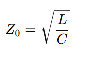
The primary goal is to preserve signal integrity while reducing loss and unwanted coupling. Unlike low-frequency designs, where DC resistance dominates, RF design must account for distributed parameters—inductance (L) and capacitance (C)—that vary along the trace.
The characteristic impedance Z0 is central to RF PCB design, defined as:
A mismatch between source and load impedances leads to reflections, quantified by the reflection coefficient:
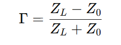
Where ZL is the load impedance. To minimize reflections and achieve efficient power transfer, ZL must closely match Z0, usually 50 Ω for most RF systems.
Key Design Principles of RF PCBs
Controlled Impedance Design
Every RF trace functions as a transmission line, not just a conductor. The impedance depends on geometry and dielectric properties. For microstrip structures, the impedance is approximated by:
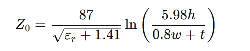
where:
- (h): dielectric height,
- (w): trace width,
- (t): copper thickness,
- εr: dielectric constant.
A deviation of even ±10% from the target impedance can distort RF signals, increasing insertion loss and reflection.
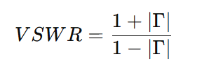
Impedance Matching
Impedance matching ensures maximum power transfer between circuit stages. When mismatch occurs, reflected energy travels back to the source, forming standing waves. The relationship between reflection coefficient and Voltage Standing Wave Ratio (VSWR) is:
In practice, designers use Smith charts, stub tuners, or LC matching networks to visualize and optimize matching.
Transmission Line Effects
At RF frequencies, traces behave like distributed elements rather than lumped components. Propagation delay, attenuation, and coupling must be analyzed using electromagnetic simulation. The wavelength λ is given by:
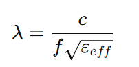
where (c) is the speed of light, (f) the frequency, and εeff the effective dielectric constant.
Material Selection for RF PCB
The choice of substrate determines dielectric stability and signal loss.
| Material | Dielectric Constant (εr) | Loss Tangent (tanδ) | Frequency Stability | Typical Use |
|---|---|---|---|---|
| FR-4 | 4.2–4.7 | 0.02 | Poor above 1 GHz | Low-cost applications |
| Rogers RO4350B | 3.48 | 0.0037 | Excellent up to 10 GHz | RF amplifiers, filters |
| PTFE (Teflon) | 2.1 | 0.0009 | Outstanding up to 30 GHz | Aerospace, radar systems |
Key considerations:
- Lower tanδ means lower dielectric loss.
- Stable εr ensures consistent impedance.
- Surface roughness of copper affects conductor loss, especially at GHz frequencies.
PCB Stack-up and Geometry
RF designs usually adopt multilayer stack-ups to separate high-frequency and control layers. A common four-layer configuration might include:
- Top Layer – RF signal traces
- Inner Layer 1 – Solid ground plane
- Inner Layer 2 – Power plane
- Bottom Layer – Control and bias circuits
Proper ground referencing is vital. The return path should be directly beneath the signal line to maintain uniform impedance. Vias must be minimized or placed symmetrically to prevent inductive discontinuities.
Differential routing is used for balanced RF lines (e.g., antennas or mixers). The differential impedance Zdiff is roughly:
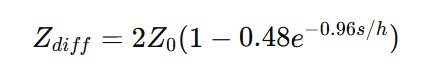
where (s) is the spacing between differential traces.
Layout and Routing Techniques
Minimizing Coupling and Crosstalk
Keep high-power and low-power RF paths separated. Perpendicular routing between layers reduces unwanted coupling.
Shielding Methods
Use guard traces and via fences around sensitive lines. Stitching vias at 1/20th wavelength intervals confine electromagnetic fields effectively.
Return Path Optimization
Ensure ground continuity with via stitching near corners or component pads. Avoid long current loops that may radiate noise.
Simulation and Testing in RF PCB Design
RF verification relies on both simulation and measurement.
- S-Parameter Analysis:
- S11: Return loss (input reflection).
- S21: Insertion loss (forward transmission).
- Ideal design targets:
- S11< -10 dB)
- S21 > -3 dB)
The Return Loss formula is:

- Time Domain Reflectometry (TDR): Detects impedance discontinuities along traces.
- Network Analyzer Testing: Validates gain, phase shift, and bandwidth performance.
Accurate measurement ensures the PCB meets design specifications before mass production.
Applications of RF Circuit PCB
RF PCBs are embedded in numerous systems:
- Wireless communication modules (Wi-Fi, Bluetooth, LTE)
- IoT sensors and gateways
- Automotive radar and collision avoidance systems
- Satellite and aerospace communication
- Medical telemetry and imaging devices
As the world transitions to 5G and beyond, RF PCB design has become central to achieving higher data rates and stable wireless connections.
Technical Capability for RF PCB Manufacturer
At EBest Circuit (Best Technology), our RF PCB manufacturing capabilities are built on nearly two decades of specialized experience in high-frequency circuit fabrication. We combine state-of-the-art equipment with rigorous quality control processes to deliver PCBs that meet the demanding requirements of modern RF applications, from 5G infrastructure to aerospace systems.
1. Precision Manufacturing with Advanced Equipment
- Laser Direct Imaging (LDI)
- Min. trace/space: 3/3 mil (standard) → 1/1 mil (advanced)
- Copper thickness: Inner layers (HOZ-20OZ) | Outer layers (1OZ-20OZ)
- Plasma Etching Systems
- Critical for RF signal integrity, supports 10:1 aspect ratio microvias and 0.15mm ultra-fine holes
2. Rigorous RF Performance Validation
- 40GHz Network Analyzers
- Direct measurement of insertion loss/return loss up to 40GHz
- Time-Domain Reflectometry (TDR)
- Full-path impedance control: ±5% (standard) | ±3% (advanced)
- Material Characterization
- Dk/Df testing for Rogers, Taconic, and other high-frequency laminates
3. RF-Optimized Material Portfolio
| Material Class | Standard Options | High-Frequency Solutions |
|---|---|---|
| FR4 | KB6165 (TG150) | Isola 370HR, FR408HR |
| High-Frequency Laminates | – | Rogers 4350/5880, Taconic TLY-5 |
| Ultra-Low Loss Materials | – | Nelco N4000-13, PTFE-based substrates |
| Dielectric Layers | 1080/2116/7628 PP | Ultra-thin cores (0.1mm, copperless) |
4. Key Process Capabilities
- Impedance Control
- Inner layers (1OZ): ±5% (4/4mil) → ±3% (3/3mil)
- High-Frequency Surface Finishes
- ENIG (Ni 3-8μm | Au 0.025-0.125μm) for mmWave applications
- Electroless NiPdAu (Pd 0.05-0.125μm) for superior solderability
5. Multilayer RF PCB Expertise
- Layer Stack-Up: 1-32 layers (High-TG mandatory for 8+ layers)
- Thickness Control:
- Ultra-thin: 0.15mm±0.05mm (ENIG only)
- Thick-board: 8.0mm (special back-drilling)
- Hybrid Construction: FR4 + Rogers material combinations
6. Scalable Production & Fast Turnkey
- Max. Panel Size: 1980mm (single/double-sided) | 750mm (multilayer)
- High-Mix Flexibility:
- Supports 2,000pcs/batch for ultra-small boards (<0.0004m²)
7. Design Support Services
- DFM (Design for Manufacturing) analysis for RF layouts
- Signal integrity and thermal management consulting
- Material selection guidance based on application requirements
- Rapid prototyping with engineering feedback within 24 hours
Through continuous investment in advanced equipment and process optimization, EBest Circuit (Best Technology) maintains its position as a leading RF PCB manufacturer capable of meeting the most demanding high-frequency application requirements.
How Do RF Laminate PCB Manufacturers Ensure Quality?
Quality in RF manufacturing is not an afterthought. It is integrated into every step. For an RF laminate PCB manufacturer, ensuring quality means controlling every variable that could affect the final electrical performance. The process is meticulous.
- Incoming Material Inspection: It starts with the raw laminate. We verify the dielectric thickness and copper cladding weight against specifications. Using a material with the wrong Dk will ruin the entire batch.
- Process Control During Fabrication: We constantly monitor critical parameters. Etching chemistry, lamination pressure and temperature, and plating thickness are all tightly controlled. This consistency is key to achieving the designed impedance.
- Electrical Testing: 100% of our RF boards undergo electrical testing. We use fixtures to test for continuity (no shorts or opens). More importantly, we sample-test boards for high-frequency parameters like impedance and loss, ensuring they meet the customer’s data sheet.
- Microsection Analysis: We regularly cross-section sample boards. This allows us to physically measure critical features: trace width, dielectric thickness, and plating quality. This data confirms our processes are in control.
This systematic approach separates a true specialist from a general-purpose fabricator. It is how we guarantee that the board you receive will perform exactly like the one you designed.
How to Select RF PCB Manufacturers?
Choosing the right partner is critical. Your RF PCB design’s success depends on their skill. Here is a simple checklist to help you select an RF PCB manufacturer.
- Proven Experience: Ask for examples of previous work. A good RF microwave PCB manufacturer will have a portfolio of projects similar to yours.
- Technical Questions: Gauge their expertise. Ask them how they control impedance or which materials they recommend for your frequency band. Their answers will reveal their depth of knowledge.
- Quality Certifications: Look for ISO 9001 certification. This shows a commitment to a documented quality management system.
- Testing Capabilities: Ensure they have the necessary equipment to verify RF performance, not just basic connectivity.
- Communication and Support: You need a responsive partner. Choose a manufacturer that assigns a dedicated engineer to your project for clear and technical communication.
Whether you are looking for an RF PCB manufacturer in the USA, China, or Europe, these core criteria remain the same. The goal is to find a partner, not just a supplier.
Case Study: RF Microwave PCB Board Manufacture by EBest Circuit (Best Technology)
Challenge: High-Frequency Signal Integrity
A 5G base station OEM required 24-layer RF microwave PCBs with:
- Strict impedance control (±3%) for 28GHz mmWave signals
- Low-loss laminate (Df <0.004) to minimize attenuation
- Plated through-holes (PTH) with 10:1 aspect ratio for dense interconnects
Our Manufacturing Solution
- Material Expertise:
- Selected Rogers 5880 (Dk=2.2, Df=0.0009) for critical RF layers
- Hybrid stack-up with FR408HR for cost-sensitive digital layers
- Advanced Processes:
- Laser-drilled microvias (0.10mm) + plasma desmear for void-free plating
- 3/3 mil trace/space with ±2μm alignment tolerance (LDI technology)
- Quality Validation:
- 40GHz network analyzer confirmed insertion loss <0.15dB/inch
- 100% TDR testing ensured impedance consistency across panels
EBest Circuit (Best Technology)’s RF Microwave PCB Capabilities
◼ Materials: Rogers, Taconic, Isola, Nelco, PTFE, and hybrid FR4 options
◼ Critical Tolerances:
- Line width/spacing: 1/1 mil (special process)
- Hole size: 0.10mm (laser) | 0.15mm (mechanical)
- Impedance control: ±3% (standard), ±2% (advanced)
◼ Testing: - 40GHz RF performance validation
- TDR, thermal cycling, IST (interconnect stress testing)
◼ Applications: 5G mmWave, satellite comms, radar, medical RF devices
In conclusion, an RF PCB manufacturer bridges the gap between high-frequency theory and real-world application. This article has explored the critical aspects that define quality in RF circuit board production. From material science to precision manufacturing, each step is vital for success.
At EBest Circuit (Best Technology), we are passionate about tackling complex RF and microwave challenges. Our expertise in RF circuit PCB design and manufacturing ensures your project is built to the highest standards. We are committed to being your reliable partner. Pls contact our team of experts at sales@bestpcbs.com for RF PCB manufacturing supports.