

The performance of an embedded copper busbar PCB depends not only on its copper thickness or geometry but also on what surrounds it. The materials and stack-up configuration are the invisible foundation that determines whether a board will stay flat, bond securely, and perform reliably under thermal stress.
When current and heat flow through thick copper blocks, the surrounding prepreg (PP) and core materials must handle mechanical pressure, resin flow, and temperature changes — all without warping or cracking. A small mismatch in materials or stack-up balance can cause delamination, resin overflow, or uneven surfaces.
At EBest Circuit (Best Technology), we’ve fine-tuned these relationships through years of building embedded copper busbar PCBs for power electronics, new energy systems, and EV modules. This guide summarizes the essential principles for selecting materials and designing the ideal lamination stack-up for embedded copper applications.
Why Material Selection Matters in Embedded Copper Busbar PCBs?
Unlike standard multilayer PCBs, an embedded copper design involves massive differences in material stiffness, density, and thermal expansion. Copper is dense and rigid, while FR-4 and PP are lighter and flexible. During lamination, heat and pressure combine these materials into one structure.
If the materials are mismatched, stress forms around the copper area. This can result in:
- Resin voids near copper corners.
- Uneven lamination pressure.
- Localized warpage after cooling.
Using the right prepreg and core ensures that the resin flows correctly, filling gaps and bonding firmly to the copper’s surface. It also ensures the copper stays perfectly aligned inside the structure.
Understanding the Core-to-Core Lamination Principle
One of the golden rules of embedded copper busbar PCB design is to use core-to-core lamination. Unlike conventional PCBs that may use copper foil on outer layers, embedded copper structures need the strength and precision of core-based lamination to prevent warping. Here’s why:
- Copper foils are too thin and flexible. When combined with thick copper blocks, they create uneven pressure.
- Core materials are dimensionally stable. They maintain thickness uniformity and resist deformation under high pressure.
- Core-to-core bonding ensures the copper block is securely enclosed by solid layers instead of loose foil and resin.
This method results in a stable, tightly bonded sandwich structure — perfect for high-current circuits.
Core Material Selection
The core material provides mechanical strength and dielectric insulation. In embedded copper designs, the core also acts as a stable base for copper slot milling and lamination.
Recommended Materials
- FR-4: The most widely used and validated material. Excellent mechanical strength and cost-effective for mass production.
- TU-872SLK, M6, SH260, FR-27, FR-28: These high-performance materials can also be used, but require non-standard validation.
- Avoid PTFE: Too soft for polishing and lamination; can deform when pressure is applied.
When polishing embedded areas, a harder surface is required to remove resin overflow without damaging the board. FR-4 performs best here, offering the perfect combination of hardness, stability, and adhesion to copper.
Prepreg (PP) Material Selection
The prepreg, or PP, acts as both the bonding medium and the gap filler between cores. It’s responsible for flowing into small spaces around the copper block during lamination and then solidifying to create strong adhesion.
For embedded copper PCBs, resin flow is critical. Low-flow materials can cause weak bonding or trapped air.
Key PP Selection Guidelines
- Use at least two PP sheets between each pair of layers.
- Choose high-resin-content PP to ensure proper filling.
- Recommended Type: Two layers of high-resin 1080PP.
- Other acceptable types: 106, 3313, 2116, 7628.
- Avoid: Rogers 4450F (poor resin flow and weak bonding strength).
Why High-Resin PP?
Because the copper block is solid and has no pores, the resin must flow into every microscopic gap along the copper edge. High-resin PP fills these spaces more effectively, creating complete contact and minimizing voids.
If the resin cannot flow freely, the interface between copper and PP may delaminate under heat cycles.
Matching PP and Core for Proper Resin Flow
The combination of PP and core thickness should complement the embedded copper thickness. If the copper block is too thick compared to the PP + core slot depth, it will create an uneven lamination surface. Thickness Correlation Guide:
| Copper Thickness (mm) | Slot Depth (PP + Core) | Resulting Copper Height After Lamination |
| 0.5–0.6 | Equal to PP + Core | Flush surface |
| 0.8 | 0–0.05mm thicker | Slightly raised |
| ≥1.0 | 0.05–0.1mm thicker | 0–0.075mm above surface |
Maintaining this relationship ensures that copper is slightly elevated after lamination, which helps transfer heat efficiently to external components.
Resin Flow and Filling Behavior
During lamination, the PP resin melts and flows around the copper block. To achieve a perfect fill, it must reach all small cavities between copper and core surfaces.
Factors That Influence Resin Flow:
- Resin content: High resin improves flowability.
- Press temperature and time: Must be controlled to prevent premature curing.
- Pressure: Enough to squeeze resin into the gaps but not too much to deform cores.
- Slot size: Should leave 0.05mm clearance on each side for resin flow.
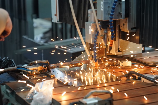
At EBest Circuit (Best Technology), engineers simulate resin flow behavior during the design stage to ensure complete encapsulation of copper. Our lamination systems monitor pressure and temperature profiles to maintain resin balance across the panel.
Copper Busbar PCBs Stack-Up Design Rules
A balanced stack-up prevents board warpage and mechanical stress. When one side of the PCB has embedded copper but the other side does not, the uneven copper distribution can lead to bowing.
To prevent this:
- Distribute embedded copper areas symmetrically when possible.
- Add dummy copper areas on the opposite side for balance.
- Use anti-warping layouts in lamination.
- Avoid placing buffer materials near copper blocks.
If balance cannot be achieved, engineers can use two release films or controlled pressure zones during lamination to keep the board flat.
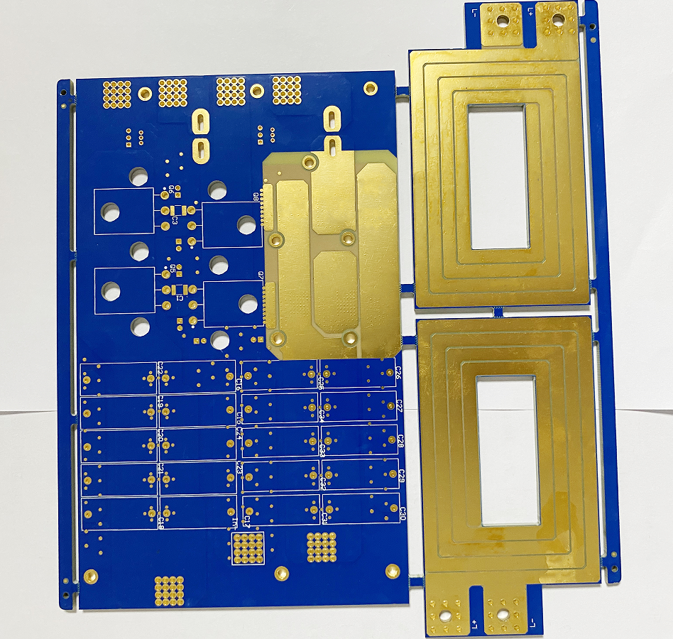
Semi-Embedded vs. Fully Embedded Stack-Up
The stack-up design also depends on whether the copper is semi-embedded or fully embedded.
Fully Embedded Stack-Up
- Copper is enclosed completely between cores.
- Surface is flat after lamination.
- Ideal for multi-layer designs or signal-integrated PCBs.
- Requires precise slot alignment on all core layers.
Semi-Embedded Stack-Up
- One side of the copper block remains exposed or nearly flush with the outer layer.
- Used when direct heat transfer is needed (e.g., under power devices).
- Must include at least one non-slotted PP layer beneath the copper block to electrically isolate it from the lower core.
Both structures rely on proper PP resin thickness to ensure even pressure and insulation between layers.
Avoiding Common Lamination Problems
Even with the right materials, poor lamination practices can compromise performance. Below are common issues and how to prevent them:
| Problem | Possible Cause | Solution |
| Resin voids around copper | Low-flow PP or tight slot fit | Use high-resin PP and add 0.05mm clearance |
| Warpage | Unbalanced copper distribution | Use symmetrical stack-up or dummy copper |
| Delamination | Poor adhesion or incomplete resin fill | Verify copper oxidation and PP quality |
| Resin overflow | Excessive resin content or pressure | Optimize PP count and press parameters |
| Surface step | Copper block too high or low | Recheck slot depth vs copper thickness |
Each of these factors can be controlled through careful material selection and process tuning.
Why Rogers 4450F Is Not Suitable as Busbar PCBs Material?
Although Rogers materials are known for high-frequency performance, Rogers 4450F PP is not suitable for embedded copper applications. Its resin flow is too low, and it bonds weakly with copper blocks.
During lamination, the limited resin mobility causes voids and poor adhesion, leading to delamination under thermal stress. For this reason, all Rogers 4450F PP designs require non-standard approval — and in most cases, alternative materials are recommended.
Dielectric and Mechanical Performance Requirements
An embedded copper PCB must maintain strong dielectric strength even with thick copper sections inside. At EBest Circuit (Best Technology), we validate dielectric and mechanical properties through standardized testing:
- Dielectric Strength: ≥ DC 1500V
- Thermal Shock Test: 288°C × 10s × 5 cycles, no delamination
- Surface Flatness: ±0.075mm
- Adhesion Test: No separation after peel strength evaluation
By using validated core and PP materials, the board can easily meet or exceed IPC-6012 performance requirements.
Engineering Tips for Material and Stack-Up Design
1. Always confirm material compatibility early in the design stage. Some special laminates require testing before production.
2. Use two or more high-resin PP layers for stable lamination around copper.
3. Keep slot clearance and copper height within specified tolerance.
4. For mixed-material designs, check CTE (coefficient of thermal expansion) compatibility to avoid stress at copper boundaries.
5. Share your stack-up drawing with the PCB supplier for DFM verification.
In our next blog, we will share the whole process of busbar PCB manufacturing, if you’re planning a new busbar PCB design, reach out to EBest Circuit (Best Technology) for expert support. Our team can help you select materials, verify manufacturability, and deliver dependable results for even the most complex embedded copper structures.
Tags: Busbar PCB, busbar pcb design